Featured post

Top 5 books to refer for a VHDL beginner

VHDL (VHSIC-HDL, Very High-Speed Integrated Circuit Hardware Description Language) is a hardware description language used in electronic des...

Sunday, 18 October 2009

Sequential Circuits


Sequential logic differs from combinational logic in that the output of the logic device is dependent not only on the present inputs to the device, but also on past inputs; i.e., the output of a sequential logic device depends on its present internal state and the present inputs. This implies that a sequential logic device has some kind of memory of at least part of its ``history'' (i.e., its previous inputs). Below figure shows a generic structure for sequential circuit.


The memory elements are devices capable of storing binary info. The binary info stored in the memory elements at any given time defines the state of the sequential circuit. The input and the present state of the memory element determines the output. Memory elements next state is also a function of external inputs and present state. A sequential circuit is specified by a time sequence of inputs, outputs, and internal states.

There are two types of sequential circuits. Their classification depends on the timing of their signals:

  • Synchronous sequential circuits
  • Asynchronous sequential circuits


  • Asynchronous sequential circuits: This is a system whose outputs depend upon the order in which its input variables change and can be affected at any instant of time.

    Gate-type asynchronous systems are basically combinational circuits with feedback paths. Because of the feedback among logic gates, the system may, at times, become unstable. Consequently they are not often used. Below is an example circuit.


    Synchronous sequential circuits:This type of system uses storage elements called flip-flops that are employed to change their binary value only at discrete instants of time. Synchronous sequential circuits use logic gates and flip-flop storage devices. Sequential circuits have a clock signal as one of their inputs. All state transitions in such circuits occur only when the clock value is either 0 or 1 or happen at the rising or falling edges of the clock depending on the type of memory elements used in the circuit. Synchronization is achieved by a timing device called a clock pulse generator. Clock pulses are distributed throughout the system in such a way that the flip-flops are affected only with the arrival of the synchronization pulse. Synchronous sequential circuits that use clock pulses in the inputs are called clocked-sequential circuits. They are stable and their timing can easily be broken down into independent discrete steps, each of which is considered separately.
    Below figure shows example circuit:


    A clock signal is a periodic square wave that indefinitely switches from 0 to 1 and from 1 to 0 at fixed intervals. Clock cycle time or clock period: the time interval between two consecutive rising or falling edges of the clock.

    Thursday, 15 October 2009

    Combinational circuits


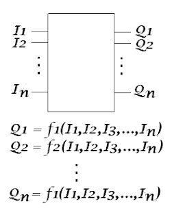
    Combinatorial Circuits are circuits which can be considered to have the following generic structure.

    Whenever the same set of inputs is fed in to a combinatorial circuit, the same outputs will be generated. Such circuits are said to be stateless. Some simple combinational logic elements that we have seen in previous sections are "Gates".
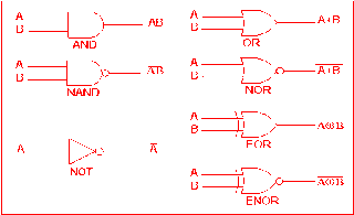
    Below figure shows the basic gates that are used to build a combinational circuit.

    Tuesday, 13 October 2009

    PCI Express: "A Layered Architecture"

    PCI Express is a layered protocol, consisting of a transaction layer, a data link layer, and a physical layer. The Data Link Layer is subdivided to include a media access control (MAC) sublayer. The Physical Layer is subdivided into logical and electrical sublayers. The Physical logical-sublayer contains a physical coding sublayer (PCS). (Terms borrowed from the IEEE 802 model of networking protocol.)

    PCI Express Layered Architecture

    Configuration/Operating System Layer —Leverages the standard mechanisms defined in the PCI Plug-and-Play specification for device initialization, enumeration, and configuration. This layer communicates with the software layer by initiating a data transfer between peripherals or receiving data from an attached peripheral. PCI Express is designed to be compatible with existing operating systems, but future operating system support is required for many of the technology’s advanced features.

    Software Layer —Generates read and write requests to peripheral devices. PCI Express maintains initialization and runtime software compatibility with PCI. Like PCI, the PCI Express initialization model allows the operating system to discover add-in hardware devices and allocate system resources. PCI Express retains the PCI configuration space and the programmability of I/O devices. In fact, all operating systems will boot without modification on a PCI Express system. The PCI runtime software model is also preserved, enabling existing software to execute unchanged.

    Transaction Layer —Transports read and write requests from the software layer to the link layer using a packet-based protocol, and matches response packets to the original software requests. The transaction layer supports 32-bit and extended 64-bit memory addressing. It also supports PCI memory, I/O, and configuration address spaces, as well as a new message space for in-band messages such as interrupts and resets. This message space eliminates the need for numerous PCI and PCI-X sideband signals.

    Link Layer —Adds sequencing and error detection cyclic redundancy codes (CRCs) to the data packets to create a reliable data transfer mechanism between the system chip set and the I/O controller.

    Physical Layer —Implements the dual simplex PCI Express channels. Implementations are flexible and various technologies and frequencies may be used. In this way, initial silicon technology can be replaced easily with future implementations that are backward compatible. For example, fiber-optic technology might be used to increase the data transfer rate.

    Mechanical Layer —Defines various form factors for peripheral devices.

    PCI Express Advanced Features

    PCI Express has advanced features that will be phased in as operating system and device support is developed and as customer applications require them:

    • Advanced power management
    • Support for real-time data traffic
    • Hot plug and hot swap
    • Data integrity and error handling

    Advanced Power Management

    PCI Express has "active-state" power management, which lowers power consumption when the bus is not active (that is, no data is being sent between components or peripherals). On a parallel interface such as PCI, no transitions occur on the interface until data needs to be sent. In contrast, high-speed serial interfaces such as PCI Express require that the interface be active at all times so that the transmitter and receiver can maintain synchronization. This is accomplished by continuously sending idle characters when there is no data to send. The receiver decodes and discards the idle characters. This process consumes additional power, which impacts battery life on portable and handheld computers.

    To address this issue, the PCI Express specification creates two low-power link states and the active-state power management (ASPM) protocol. When the PCI Express link goes idle, the link can transition to one of the two low-power states. These states save power when the link is idle, but require a recovery time to resynchronize the transmitter and receiver when data needs to be transmitted. The longer the recovery time (or latency), the lower the power usage. The most frequent implementation will be the low-power state with the shortest recovery time.

    Support for Real-Time Data Traffic

    Unlike PCI, PCI Express includes native support for isochronous (or time-dependent) data transfers and various QoS levels. These features are implemented via "virtual channels" that are designed to guarantee that particular data packets arrive at their destination in a given period of time. PCI Express supports multiple isochronous virtual channels—each an independent communications session—per lane. Each channel may have a different QoS level. This end-to-end solution is designed for applications that require real-time delivery such as real-time voice and video.

    Hot Plug and Hot Swap

    PCI-based systems do not have native (or built-in) support for hot plugging or hot swapping I/O cards. Instead, a few limited server and PC Card hot plug, hot swap implementations were developed as add-ons to PCI after the original bus definition. These solutions addressed pressing requirements of server and portable computer platforms:

    • It is often difficult or impossible to schedule downtime on a server to replace or install peripheral cards. The ability to hot plug I/O devices minimizes downtime.
    • Portable computer users need the ability to hot plug cards that provide I/O functions such as mobile disk drives and communications.

    PCI Express has native support for hot plugging and hot swapping I/O peripherals. No sideband signals are required and a unified software model can be used for all PCI Express form factors.

    Data Integrity and Error Handling

    PCI Express supports link-level data integrity for all types of transaction- and data-link packets. Thus, it is suitable for end-to-end data integrity for high-availability applications, particularly those running on server systems. PCI Express also supports PCI error handling and has advanced error reporting and handling to help improve fault isolation and recovery solutions.

    Data Transfer Rates In PCIe


    The bandwidth of a PCI Express link can be scaled by adding signal pairs to form multiple lanes between the two devices. The specification supports x1, x4, x8, and x16 lane widths and stripes the byte data across the links accordingly. Once the two agents at each end of the PCI Express link negotiate lane widths and frequency of operation, the striped data bytes are transmitted with 8b/10b encoding.
    The basic "x1" link has a peak raw bandwidth of 2.5 Gbps. Because the bus is bidirectional (that is, data can be transferred in both directions simultaneously), the effective raw data transfer rate is 5 Gbps. Table below summarizes the encoded and unencoded data rates of x1, x4, x8, and x16 implementations, which are defined in the initial generation of PCI Express.

    Table: PCI Express Bandwidth


    In contrast to PCI, PCI Express has minimal sideband signals and the clocks and addressing information are embedded in the data. Because PCI Express is a serial technology with few sideband signals, it provides a very high bandwidth per I/O connector pin compared to PCI. This is designed to result in more efficient, smaller, and cheaper connectors. Figure below compares the bandwidth per I/O connector pin of PCI, PCI-X, AGP, and PCI Express.Future implementations of PCI Express will raise the channel communication frequency to even higher levels. For example, a second generation of PCI Express could increase the communication frequency by a factor of 2 or more.
    Because it is a point-to-point architecture, the entire bandwidth of each PCI Express bus is dedicated to the device at the end of the link. Multiple PCI Express devices can be active without interfering with each other.
    Figure 5. Comparison of I/O Bus Bandwidth Per Pin
    Figure. Comparison of I/O Bus Bandwidth Per Pin
    PCI Express technology achieves high data rates reliably by using low-voltage differential signaling. In this approach, the signal is sent from the source to the receiver over two lines. One contains a "positive" image and the other, a "negative" or "inverted" image of the signal. The lines are routed using strict routing rules so that any noise that affects one line also affects the other line. The receiver collects both signals, inverts the negative version back to the positive and sums the two collected signals, which effectively removes the noise.
    The original PCI Express specification defines graphics cards with up to 75 watts of power. In addition, a new high-end PCI Express graphics specification is under development that defines cards of up to 150 watts. These higher power levels accommodate the requirements of graphics adapters, which currently peak at 41 watts for mainstream AGP cards and 110 watts for AGP Pro 110 cards.

    Key Features Of PCIe

    • Compatible with the current PCI software model: There are no changes required to the current Operating Systems while maintaining platform configuration and device driver interfaces. Enables smooth integration within future system allowing for broad industry adoption.

    • Serial architecture; Low-pin-count point-to-point connection (link): Does away with some of the limitations of parallel bus architectures by using embedded clock timing and differential signaling. The embedded clock lowers pin count (no separate control and clock pins are required) and makes data synchronization easier than in a parallel-based technology. Data can traverse a connector and cable scheme allowing flexible system partitioning. Serial technology enables unique and small form factors, reduces cost, simplifies board design and routing and reduces signal integrity issues. Point-to-point interconnect means no multiple hosts on same bus creating a bottleneck.
    • Bandwidth scalability and frequency and/or interconnect width:Each link can be scalable up in bandwidth by creating wider lanes to match applications use, such as a wider graphics port in Desktop or multiple bus bridges (PCI Express-to-PCI-X, -Gigabit Ethernet or - InfiniBand) in server platforms. The spec defines interface widths of x1, x2, x4, x8, x12, x16 or x32 lanes.

    • Embedded clock or CDR (Clock Data Recovery): Lowers pin counts, enables superior frequency scalability versus source synchronous clocking, and makes data synchronization easier.

    • Layered architecture: The architecture consisting of the Software layer, Transaction Layer, Data Link Layer and Physical Layer. Layering enables scalability, modularity and design reuse.

    • Packetized protocol: Time multiplexing versus circuit switching. This allows more than two-way communication at one time unlike circuit switching where only a two-way communications can occur. With packet based protocol there is no wasted bandwidth.

    • Advanced features: Aggressive power management, QoS, isochrony, hot attach/detach and RAS.

    Digital Design

    As i have mentioned earlier that digital design concepts has to be crystal clear while you design a digital circuit. Here we will stat with the basic concepts of digital designing.

    Digital or binary logic has fascinated many people over the years. The very idea that a two-valued number system can possibly be the basis for the most powerful and sophisticated computers seems astounding, to say the least. Nevertheless, it is so, and the how and the why of this requires some explanation.

    Everything in the digital world is based on the binary number system. Numerically, this involves only two symbols: 0 and 1. Logically, we can use these symbols or we can equate them with others according to the needs of the moment. Thus, when dealing with digital logic, we can specify that:

    0 = false = no
    1 = true = yes

    Using this two-valued logic system, every statement or condition must be either "true" or "false;" it cannot be partly true and partly false. While this approach may seem limited, it actually works quite nicely, and can be expanded to express very complex relationships and interactions among any number of individual conditions.

    Digital logic may be divided into two classes:

    => combinational logic, in which the logical outputs are determined by the logical function being performed and the logical input states at that particular moment. A simple combinational circuit is shown below.


    =>sequential logic, in which the outputs also depend on the prior states of those outputs. Both classes of logic are used extensively in all digital computers. A Latch is considered to be a simplest sequential circuit. A simple sequential circuit is shown below.