Featured post

Top 5 books to refer for a VHDL beginner

VHDL (VHSIC-HDL, Very High-Speed Integrated Circuit Hardware Description Language) is a hardware description language used in electronic des...

Tuesday, 13 October 2009

PCI Express Advanced Features

PCI Express has advanced features that will be phased in as operating system and device support is developed and as customer applications require them:

  • Advanced power management
  • Support for real-time data traffic
  • Hot plug and hot swap
  • Data integrity and error handling

Advanced Power Management

PCI Express has "active-state" power management, which lowers power consumption when the bus is not active (that is, no data is being sent between components or peripherals). On a parallel interface such as PCI, no transitions occur on the interface until data needs to be sent. In contrast, high-speed serial interfaces such as PCI Express require that the interface be active at all times so that the transmitter and receiver can maintain synchronization. This is accomplished by continuously sending idle characters when there is no data to send. The receiver decodes and discards the idle characters. This process consumes additional power, which impacts battery life on portable and handheld computers.

To address this issue, the PCI Express specification creates two low-power link states and the active-state power management (ASPM) protocol. When the PCI Express link goes idle, the link can transition to one of the two low-power states. These states save power when the link is idle, but require a recovery time to resynchronize the transmitter and receiver when data needs to be transmitted. The longer the recovery time (or latency), the lower the power usage. The most frequent implementation will be the low-power state with the shortest recovery time.

Support for Real-Time Data Traffic

Unlike PCI, PCI Express includes native support for isochronous (or time-dependent) data transfers and various QoS levels. These features are implemented via "virtual channels" that are designed to guarantee that particular data packets arrive at their destination in a given period of time. PCI Express supports multiple isochronous virtual channels—each an independent communications session—per lane. Each channel may have a different QoS level. This end-to-end solution is designed for applications that require real-time delivery such as real-time voice and video.

Hot Plug and Hot Swap

PCI-based systems do not have native (or built-in) support for hot plugging or hot swapping I/O cards. Instead, a few limited server and PC Card hot plug, hot swap implementations were developed as add-ons to PCI after the original bus definition. These solutions addressed pressing requirements of server and portable computer platforms:

  • It is often difficult or impossible to schedule downtime on a server to replace or install peripheral cards. The ability to hot plug I/O devices minimizes downtime.
  • Portable computer users need the ability to hot plug cards that provide I/O functions such as mobile disk drives and communications.

PCI Express has native support for hot plugging and hot swapping I/O peripherals. No sideband signals are required and a unified software model can be used for all PCI Express form factors.

Data Integrity and Error Handling

PCI Express supports link-level data integrity for all types of transaction- and data-link packets. Thus, it is suitable for end-to-end data integrity for high-availability applications, particularly those running on server systems. PCI Express also supports PCI error handling and has advanced error reporting and handling to help improve fault isolation and recovery solutions.
Data Transfer Rates In PCIe


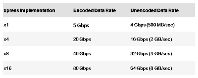
The bandwidth of a PCI Express link can be scaled by adding signal pairs to form multiple lanes between the two devices. The specification supports x1, x4, x8, and x16 lane widths and stripes the byte data across the links accordingly. Once the two agents at each end of the PCI Express link negotiate lane widths and frequency of operation, the striped data bytes are transmitted with 8b/10b encoding.
The basic "x1" link has a peak raw bandwidth of 2.5 Gbps. Because the bus is bidirectional (that is, data can be transferred in both directions simultaneously), the effective raw data transfer rate is 5 Gbps. Table below summarizes the encoded and unencoded data rates of x1, x4, x8, and x16 implementations, which are defined in the initial generation of PCI Express.

Table: PCI Express Bandwidth


In contrast to PCI, PCI Express has minimal sideband signals and the clocks and addressing information are embedded in the data. Because PCI Express is a serial technology with few sideband signals, it provides a very high bandwidth per I/O connector pin compared to PCI. This is designed to result in more efficient, smaller, and cheaper connectors. Figure below compares the bandwidth per I/O connector pin of PCI, PCI-X, AGP, and PCI Express.Future implementations of PCI Express will raise the channel communication frequency to even higher levels. For example, a second generation of PCI Express could increase the communication frequency by a factor of 2 or more.
Because it is a point-to-point architecture, the entire bandwidth of each PCI Express bus is dedicated to the device at the end of the link. Multiple PCI Express devices can be active without interfering with each other.
Figure 5. Comparison of I/O Bus Bandwidth Per Pin
Figure. Comparison of I/O Bus Bandwidth Per Pin
PCI Express technology achieves high data rates reliably by using low-voltage differential signaling. In this approach, the signal is sent from the source to the receiver over two lines. One contains a "positive" image and the other, a "negative" or "inverted" image of the signal. The lines are routed using strict routing rules so that any noise that affects one line also affects the other line. The receiver collects both signals, inverts the negative version back to the positive and sums the two collected signals, which effectively removes the noise.
The original PCI Express specification defines graphics cards with up to 75 watts of power. In addition, a new high-end PCI Express graphics specification is under development that defines cards of up to 150 watts. These higher power levels accommodate the requirements of graphics adapters, which currently peak at 41 watts for mainstream AGP cards and 110 watts for AGP Pro 110 cards.

Key Features Of PCIe

  • Compatible with the current PCI software model: There are no changes required to the current Operating Systems while maintaining platform configuration and device driver interfaces. Enables smooth integration within future system allowing for broad industry adoption.

  • Serial architecture; Low-pin-count point-to-point connection (link): Does away with some of the limitations of parallel bus architectures by using embedded clock timing and differential signaling. The embedded clock lowers pin count (no separate control and clock pins are required) and makes data synchronization easier than in a parallel-based technology. Data can traverse a connector and cable scheme allowing flexible system partitioning. Serial technology enables unique and small form factors, reduces cost, simplifies board design and routing and reduces signal integrity issues. Point-to-point interconnect means no multiple hosts on same bus creating a bottleneck.
  • Bandwidth scalability and frequency and/or interconnect width:Each link can be scalable up in bandwidth by creating wider lanes to match applications use, such as a wider graphics port in Desktop or multiple bus bridges (PCI Express-to-PCI-X, -Gigabit Ethernet or - InfiniBand) in server platforms. The spec defines interface widths of x1, x2, x4, x8, x12, x16 or x32 lanes.

  • Embedded clock or CDR (Clock Data Recovery): Lowers pin counts, enables superior frequency scalability versus source synchronous clocking, and makes data synchronization easier.

  • Layered architecture: The architecture consisting of the Software layer, Transaction Layer, Data Link Layer and Physical Layer. Layering enables scalability, modularity and design reuse.

  • Packetized protocol: Time multiplexing versus circuit switching. This allows more than two-way communication at one time unlike circuit switching where only a two-way communications can occur. With packet based protocol there is no wasted bandwidth.

  • Advanced features: Aggressive power management, QoS, isochrony, hot attach/detach and RAS.

Digital Design

As i have mentioned earlier that digital design concepts has to be crystal clear while you design a digital circuit. Here we will stat with the basic concepts of digital designing.

Digital or binary logic has fascinated many people over the years. The very idea that a two-valued number system can possibly be the basis for the most powerful and sophisticated computers seems astounding, to say the least. Nevertheless, it is so, and the how and the why of this requires some explanation.

Everything in the digital world is based on the binary number system. Numerically, this involves only two symbols: 0 and 1. Logically, we can use these symbols or we can equate them with others according to the needs of the moment. Thus, when dealing with digital logic, we can specify that:

0 = false = no
1 = true = yes

Using this two-valued logic system, every statement or condition must be either "true" or "false;" it cannot be partly true and partly false. While this approach may seem limited, it actually works quite nicely, and can be expanded to express very complex relationships and interactions among any number of individual conditions.

Digital logic may be divided into two classes:

=> combinational logic, in which the logical outputs are determined by the logical function being performed and the logical input states at that particular moment. A simple combinational circuit is shown below.


=>sequential logic, in which the outputs also depend on the prior states of those outputs. Both classes of logic are used extensively in all digital computers. A Latch is considered to be a simplest sequential circuit. A simple sequential circuit is shown below.


Sunday, 13 September 2009

Very Large Scale Integration

Hi everybody, before starting i would like to say that i have started this blog to share my experiences in VLSI designing which can be helpful to the students and engineers who wants to enter into one of the evergreen and royal field of electronics.

Most of the students of Electronics Engineering are exposed to Integrated Circuits (IC's) at a very basic level, involving SSI (small scale integration) circuits like logic gates or MSI (medium scale integration) circuits like multiplexers, parity encoders etc. But there is a lot bigger world out there involving miniaturization at levels so great, that a micrometer and a microsecond are literally considered huge! This is the world of VLSI - Very Large Scale Integration. The article aims at trying to introduce Electronics Engineering students to the possibilities and the work involved in this field.

VLSI stands for "Very Large Scale Integration”. This is the field which involves packing more and more logic devices into smaller and smaller areas. Thanks to VLSI, circuits that would have taken boards full space can now be put into a small space few millimeters across! This has opened up a big opportunity to do things that were not possible before. VLSI circuits are everywhere ... your computer, your car, your brand new state-of-the-art digital camera, the cell-phones, and what have you. All this involves a lot of expertise on many fronts within the same field.

A typical digital design flow is as follows:

Specification =>Architecture =>RTL Coding =>RTL Verification =>Synthesis =>Backend =>Tape Out to Foundry to get end product….a wafer with repeated number of identical Ics.

All modern digital designs start with a designer writing a hardware description of the IC (using HDL or Hardware Description Language) in Verilog/VHDL. A Verilog or VHDL program essentially describes the hardware (logic gates, Flip-Flops, counters etc) and the interconnect of the circuit blocks and the functionality. Various CAD tools are available to synthesize a circuit based on the HDL. The most widely used synthesis tools come from two CAD companies, Synposys and Cadence.

Without going into details, we can say that the VHDL can be called as the "C" of the VLSI industry. VHDL stands for "VHSIC Hardware Definition Language", where VHSIC stands for "Very High Speed Integrated Circuit". This language is used to design the circuits at a high-level, in two ways. It can either be a behavioral description, which describes what the circuit is supposed to do, or a structural description, which describes what the circuit is made of. There are other languages for describing circuits, such as Verilog, which work in a similar fashion.

Both forms of description are then used to generate a very low-level description that actually spells out how all this is to be fabricated on the silicon chips. This will result in the manufacture of the intended IC.

A typical analog design flow is as follows:


In case of analog design, the flow changes somewhat.

=>Specifications=> Architecture =>Circuit Design =>SPICE Simulation =>Layout =>Parametric Extraction / Back Annotation =>Final Design =>Tape Out to foundry.

While digital design is highly automated now, very small portion of analog design can be automated. There is a hardware description language called AHDL but is not widely used as it does not accurately give us the behavioral model of the circuit because of the complexity of the effects of parasitic on the analog behavior of the circuit. Many analog chips are what are termed as “flat” or non-hierarchical designs. This is true for small transistor count chips such as an operational amplifier, or a filter or a power management chip. For more complex analog chips such as data converters, the design is done at a transistor level, building up to a cell level, then a block level and then integrated at a chip level. Not many CAD tools are available for analog design even today and thus analog design remains a difficult art. SPICE remains the most useful simulation tool for analog as well as digital design.

From above discussion n from my personal experience i feel that digital design is the most important aspect of the VLSI design flow. Think if your design has some bug...!! the whole process then is costing billions of $. So it's very essential to take care start from the initial phase of designing.

Here during our discussion further we will go through several important concepts of digital dsigning and also see some standard designs.

Friday, 19 June 2009

Overview


PCI Express has generated a lot of excitement in the PC enthusiast scene in a short amount of time. And with good reason, since it promises to rid the PC of its bandwidth woes and enable a new class of applications.

Conceptually, the PCIe bus can be thought of as a high-speed serial replacement of the older (parallel) PCI/PCI-X bus. At the software-level, PCIe preserves compatibility with PCI; a PCIe device can be configured and used in legacy applications and operating-systems which have no direct knowledge of PCIe's newer features. In terms of bus-protocol, PCIe communication is encapsulated in packets.
As shown in Figure , PCI Express unifies the I/O system using a common bus architecture. In addition, PCI Express replaces some of the internal buses that link subsystems.


This third-generation I/O technology is needed today since PCI-based shared, parallel-bus-signaling technology is approaching its practical performance limits; it is increasingly difficult to scale-up bandwidth just by increasing the number of signal lines. More signal lines mean difficult clock-to-data skew management, creating complex PCB layout rules that make cost-effective implementations in the FR4 (current copper PCB) technology difficult. In addition, increasing the number of signal lines also increases the power dissipation. PCI Express allows for very high available bandwidth per pin with the ability to cost-effectively scale towards the 12 GHz limits of copper signaling technology.

PCI Express is designed to be a general-purpose serial I/O interconnect that can be used in multiple market segments, including desktop, mobile, server, storage and embedded communications. PCI Express can be used as a peripheral device interconnect, a chip-to-chip interconnect, and a bridge to other interconnects like 1394b, USB2.0, InifiniBand™ and Ethernet. It can also be used in graphics chipsets for increased graphics bandwidth.

PCI Express

There are certain times in the evolution of technology that serve as inflection points that forever change the course of events. For the computing sector and communications, the adoption of PCI Express, a groundbreaking new general input/output architecture, will serve as one of these inflection points. PCI Express allows computers to evolve far beyond their current infrastructure. In addition to this, PCI Express provides many new and exciting features such as Active Power Management, Quality of Service, Hot Plug and Hot Swap support and true isochronous capabilities.