PCI Express has advanced features that will be phased in as operating system and device support is developed and as customer applications require them:
- Advanced power management
- Support for real-time data traffic
- Hot plug and hot swap
- Data integrity and error handling
|
Advanced Power Management
PCI Express has "active-state" power management, which lowers power consumption when the bus is not active (that is, no data is being sent between components or peripherals). On a parallel interface such as PCI, no transitions occur on the interface until data needs to be sent. In contrast, high-speed serial interfaces such as PCI Express require that the interface be active at all times so that the transmitter and receiver can maintain synchronization. This is accomplished by continuously sending idle characters when there is no data to send. The receiver decodes and discards the idle characters. This process consumes additional power, which impacts battery life on portable and handheld computers.
To address this issue, the PCI Express specification creates two low-power link states and the active-state power management (ASPM) protocol. When the PCI Express link goes idle, the link can transition to one of the two low-power states. These states save power when the link is idle, but require a recovery time to resynchronize the transmitter and receiver when data needs to be transmitted. The longer the recovery time (or latency), the lower the power usage. The most frequent implementation will be the low-power state with the shortest recovery time.
Support for Real-Time Data Traffic
Unlike PCI, PCI Express includes native support for isochronous (or time-dependent) data transfers and various QoS levels. These features are implemented via "virtual channels" that are designed to guarantee that particular data packets arrive at their destination in a given period of time. PCI Express supports multiple isochronous virtual channels—each an independent communications session—per lane. Each channel may have a different QoS level. This end-to-end solution is designed for applications that require real-time delivery such as real-time voice and video.
Hot Plug and Hot Swap
PCI-based systems do not have native (or built-in) support for hot plugging or hot swapping I/O cards. Instead, a few limited server and PC Card hot plug, hot swap implementations were developed as add-ons to PCI after the original bus definition. These solutions addressed pressing requirements of server and portable computer platforms:
- It is often difficult or impossible to schedule downtime on a server to replace or install peripheral cards. The ability to hot plug I/O devices minimizes downtime.
- Portable computer users need the ability to hot plug cards that provide I/O functions such as mobile disk drives and communications.
|
PCI Express has native support for hot plugging and hot swapping I/O peripherals. No sideband signals are required and a unified software model can be used for all PCI Express form factors.
Data Integrity and Error Handling
PCI Express supports link-level data integrity for all types of transaction- and data-link packets. Thus, it is suitable for end-to-end data integrity for high-availability applications, particularly those running on server systems. PCI Express also supports PCI error handling and has advanced error reporting and handling to help improve fault isolation and recovery solutions.
 Whenever the same set of inputs is fed in to a combinatorial circuit, the same outputs will be generated. Such circuits are said to be stateless. Some simple combinational logic elements that we have seen in previous sections are "Gates".
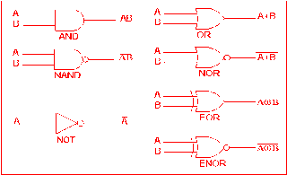


