XNOR gates have two bits of input and a single bit of output.
The output of XNOR gate is the negation of XOR and has logic '1' when both inputs are the same.

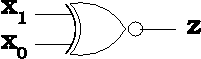
If you look carefully at the drawing of the gate, there is a second arc behind the first one near the inputs. Since this second arc is hard to see, it's usually a good idea to write the word "XNOR" inside the gate.
The truth table defines the behavior of this gate.


The function implmented by XNOR gates has interesting properties:
The function is symmetric. Thus, x XNOR y == y XNOR x. This can be verified by using truth tables.
The function is associative. Thus, (x XNOR y) XNOR z == x XNOR (y XNOR z). This can be verified by using truth tables.
Because of these properties, it's easy to define XNORn, which is an n-input XNOR gate.
XNORn(x1, x2,...,xn) = x1 XNOR x2 XNOR ... XNOR xn
That is, an XNOR gate with n-inputs is the XNOR of all the bits. This is not ambiguous because the XNOR function is associative (all parenthesization of this expression are equivalent).
(Error-checkers! You may wish to verify this, and email me if this is incorrect!).


