Featured post

Top 5 books to refer for a VHDL beginner

VHDL (VHSIC-HDL, Very High-Speed Integrated Circuit Hardware Description Language) is a hardware description language used in electronic des...

Friday, 18 December 2009

Intel Unveils 32nm Chips

Intel on Thursday said it is in volume production of its next-generation 32-nanometer desktop and laptop chips, with products available for low-end, mainstream and high-end PCs.

A total of 17 new CPUs, along with three new chipsets and seven chips providing Wi-Fi and WiMax support, will be available in computer makers' products early next year, following the International Consumer Electronics Show in January, Intel executives said during a news conference in San Francisco. The new products will be in computers covering 400 separate designs.


All the new products are built using Intel's next-generation 32-nanometer technology, codenamed Westmere, and are based on the Nehalem microarchitecture. The brands are Core i3 for low-end systems, Core i5 for mainstream PCs and Core i7 for the highest end computers used in video editing and playing top-of-the line video games. Intel started shipping 32-nanometer processors this year, but the upcoming products are the first to cover all PC categories.

The Core i7 processors, codenamed Lynnfield for the desktop models and Clarksfield for the laptop versions, are all quad-core processors. The i5 processors are available in quad-core and dual-core models, and the i3 are only dual-core.

All of the dual-core processors have the CPU and graphics processor integrated on a single die, with the memory controller on a separate chip. Previous generations had each of the three components on a separate die. The Core i7 products, which are typically used in systems with a separate graphics card, do not have integrated graphics, which Intel now calls its HD (high-definition) Graphics. Previously, Intel called its graphics technology GMA for graphics media accelerator.

Intel says its latest graphics technology is better than the previous generation because more of the work is done on the hardware versus software. As a result, end users will see smoother, sharper and more colorful playback of Blu-ray video and DVDs. The same is true for picture-in-picture playback, according to Intel.

In addition, Intel graphics support multiple monitors and DisplayPort and Dual HDMI interfaces. The former is used to connect to monitors and home-theater systems and the latter to audio/video devices, such as Blu-ray disc players, set-top boxes and video-game consoles.

The Core i5 and i7 products will all have Intel's Turbo-Boost technology, which ratchets up processing power to meet workload bursts and then lowers it when extra horsepower is no longer needed. The technology also has what Intel calls "power-gating," which will leave idle all cores that aren't needed to accomplish particular tasks. Turbo-Boost technology in general makes processors more efficient in terms of energy use.

Intel plans to release pricing and further details on the new products at CES, which runs from Jan. 7-10 in Las Vegas, Nev.

Intel unveiled its new line the same day researcher IDC released an upbeat report on the PC market. The analyst firm said the overall market in terms of shipments returned to year-over-year growth in the third quarter after three consecutive quarters of decline. Starting next year, IDC says shipments will increase in the low double-digits through 2013.

While facing a brighter outlook for the PC industry, Intel is looking at dark clouds on the legal front. The chipmaker is dealing with increasing pressure from government agencies in and outside the U.S. that accuse the company of anti-competitive behavior. Intel's latest legal headache came this week from the Federal Trade Commission, which used the company, claiming it uses its dominance to stifle competition.


Sunday, 18 October 2009

Sequential Circuits


Sequential logic differs from combinational logic in that the output of the logic device is dependent not only on the present inputs to the device, but also on past inputs; i.e., the output of a sequential logic device depends on its present internal state and the present inputs. This implies that a sequential logic device has some kind of memory of at least part of its ``history'' (i.e., its previous inputs). Below figure shows a generic structure for sequential circuit.


The memory elements are devices capable of storing binary info. The binary info stored in the memory elements at any given time defines the state of the sequential circuit. The input and the present state of the memory element determines the output. Memory elements next state is also a function of external inputs and present state. A sequential circuit is specified by a time sequence of inputs, outputs, and internal states.

There are two types of sequential circuits. Their classification depends on the timing of their signals:

  • Synchronous sequential circuits
  • Asynchronous sequential circuits


  • Asynchronous sequential circuits: This is a system whose outputs depend upon the order in which its input variables change and can be affected at any instant of time.

    Gate-type asynchronous systems are basically combinational circuits with feedback paths. Because of the feedback among logic gates, the system may, at times, become unstable. Consequently they are not often used. Below is an example circuit.


    Synchronous sequential circuits:This type of system uses storage elements called flip-flops that are employed to change their binary value only at discrete instants of time. Synchronous sequential circuits use logic gates and flip-flop storage devices. Sequential circuits have a clock signal as one of their inputs. All state transitions in such circuits occur only when the clock value is either 0 or 1 or happen at the rising or falling edges of the clock depending on the type of memory elements used in the circuit. Synchronization is achieved by a timing device called a clock pulse generator. Clock pulses are distributed throughout the system in such a way that the flip-flops are affected only with the arrival of the synchronization pulse. Synchronous sequential circuits that use clock pulses in the inputs are called clocked-sequential circuits. They are stable and their timing can easily be broken down into independent discrete steps, each of which is considered separately.
    Below figure shows example circuit:


    A clock signal is a periodic square wave that indefinitely switches from 0 to 1 and from 1 to 0 at fixed intervals. Clock cycle time or clock period: the time interval between two consecutive rising or falling edges of the clock.

    Thursday, 15 October 2009

    Combinational circuits


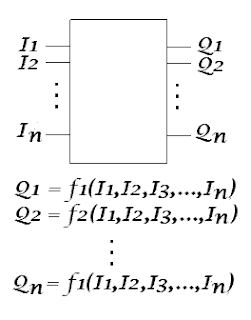
    Combinatorial Circuits are circuits which can be considered to have the following generic structure.

    Whenever the same set of inputs is fed in to a combinatorial circuit, the same outputs will be generated. Such circuits are said to be stateless. Some simple combinational logic elements that we have seen in previous sections are "Gates".

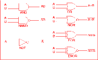
    Below figure shows the basic gates that are used to build a combinational circuit.

    Tuesday, 13 October 2009

    PCI Express: "A Layered Architecture"

    PCI Express is a layered protocol, consisting of a transaction layer, a data link layer, and a physical layer. The Data Link Layer is subdivided to include a media access control (MAC) sublayer. The Physical Layer is subdivided into logical and electrical sublayers. The Physical logical-sublayer contains a physical coding sublayer (PCS). (Terms borrowed from the IEEE 802 model of networking protocol.)

    PCI Express Layered Architecture

    Configuration/Operating System Layer —Leverages the standard mechanisms defined in the PCI Plug-and-Play specification for device initialization, enumeration, and configuration. This layer communicates with the software layer by initiating a data transfer between peripherals or receiving data from an attached peripheral. PCI Express is designed to be compatible with existing operating systems, but future operating system support is required for many of the technology’s advanced features.

    Software Layer —Generates read and write requests to peripheral devices. PCI Express maintains initialization and runtime software compatibility with PCI. Like PCI, the PCI Express initialization model allows the operating system to discover add-in hardware devices and allocate system resources. PCI Express retains the PCI configuration space and the programmability of I/O devices. In fact, all operating systems will boot without modification on a PCI Express system. The PCI runtime software model is also preserved, enabling existing software to execute unchanged.

    Transaction Layer —Transports read and write requests from the software layer to the link layer using a packet-based protocol, and matches response packets to the original software requests. The transaction layer supports 32-bit and extended 64-bit memory addressing. It also supports PCI memory, I/O, and configuration address spaces, as well as a new message space for in-band messages such as interrupts and resets. This message space eliminates the need for numerous PCI and PCI-X sideband signals.

    Link Layer —Adds sequencing and error detection cyclic redundancy codes (CRCs) to the data packets to create a reliable data transfer mechanism between the system chip set and the I/O controller.

    Physical Layer —Implements the dual simplex PCI Express channels. Implementations are flexible and various technologies and frequencies may be used. In this way, initial silicon technology can be replaced easily with future implementations that are backward compatible. For example, fiber-optic technology might be used to increase the data transfer rate.

    Mechanical Layer —Defines various form factors for peripheral devices.

    PCI Express Advanced Features

    PCI Express has advanced features that will be phased in as operating system and device support is developed and as customer applications require them:

    • Advanced power management
    • Support for real-time data traffic
    • Hot plug and hot swap
    • Data integrity and error handling

    Advanced Power Management

    PCI Express has "active-state" power management, which lowers power consumption when the bus is not active (that is, no data is being sent between components or peripherals). On a parallel interface such as PCI, no transitions occur on the interface until data needs to be sent. In contrast, high-speed serial interfaces such as PCI Express require that the interface be active at all times so that the transmitter and receiver can maintain synchronization. This is accomplished by continuously sending idle characters when there is no data to send. The receiver decodes and discards the idle characters. This process consumes additional power, which impacts battery life on portable and handheld computers.

    To address this issue, the PCI Express specification creates two low-power link states and the active-state power management (ASPM) protocol. When the PCI Express link goes idle, the link can transition to one of the two low-power states. These states save power when the link is idle, but require a recovery time to resynchronize the transmitter and receiver when data needs to be transmitted. The longer the recovery time (or latency), the lower the power usage. The most frequent implementation will be the low-power state with the shortest recovery time.

    Support for Real-Time Data Traffic

    Unlike PCI, PCI Express includes native support for isochronous (or time-dependent) data transfers and various QoS levels. These features are implemented via "virtual channels" that are designed to guarantee that particular data packets arrive at their destination in a given period of time. PCI Express supports multiple isochronous virtual channels—each an independent communications session—per lane. Each channel may have a different QoS level. This end-to-end solution is designed for applications that require real-time delivery such as real-time voice and video.

    Hot Plug and Hot Swap

    PCI-based systems do not have native (or built-in) support for hot plugging or hot swapping I/O cards. Instead, a few limited server and PC Card hot plug, hot swap implementations were developed as add-ons to PCI after the original bus definition. These solutions addressed pressing requirements of server and portable computer platforms:

    • It is often difficult or impossible to schedule downtime on a server to replace or install peripheral cards. The ability to hot plug I/O devices minimizes downtime.
    • Portable computer users need the ability to hot plug cards that provide I/O functions such as mobile disk drives and communications.

    PCI Express has native support for hot plugging and hot swapping I/O peripherals. No sideband signals are required and a unified software model can be used for all PCI Express form factors.

    Data Integrity and Error Handling

    PCI Express supports link-level data integrity for all types of transaction- and data-link packets. Thus, it is suitable for end-to-end data integrity for high-availability applications, particularly those running on server systems. PCI Express also supports PCI error handling and has advanced error reporting and handling to help improve fault isolation and recovery solutions.

    Data Transfer Rates In PCIe


    The bandwidth of a PCI Express link can be scaled by adding signal pairs to form multiple lanes between the two devices. The specification supports x1, x4, x8, and x16 lane widths and stripes the byte data across the links accordingly. Once the two agents at each end of the PCI Express link negotiate lane widths and frequency of operation, the striped data bytes are transmitted with 8b/10b encoding.
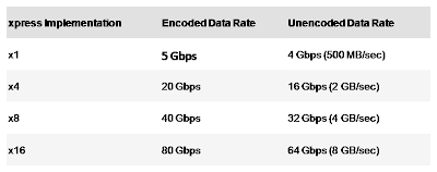
    The basic "x1" link has a peak raw bandwidth of 2.5 Gbps. Because the bus is bidirectional (that is, data can be transferred in both directions simultaneously), the effective raw data transfer rate is 5 Gbps. Table below summarizes the encoded and unencoded data rates of x1, x4, x8, and x16 implementations, which are defined in the initial generation of PCI Express.

    Table: PCI Express Bandwidth


    In contrast to PCI, PCI Express has minimal sideband signals and the clocks and addressing information are embedded in the data. Because PCI Express is a serial technology with few sideband signals, it provides a very high bandwidth per I/O connector pin compared to PCI. This is designed to result in more efficient, smaller, and cheaper connectors. Figure below compares the bandwidth per I/O connector pin of PCI, PCI-X, AGP, and PCI Express.Future implementations of PCI Express will raise the channel communication frequency to even higher levels. For example, a second generation of PCI Express could increase the communication frequency by a factor of 2 or more.
    Because it is a point-to-point architecture, the entire bandwidth of each PCI Express bus is dedicated to the device at the end of the link. Multiple PCI Express devices can be active without interfering with each other.
    Figure 5. Comparison of I/O Bus Bandwidth Per Pin
    Figure. Comparison of I/O Bus Bandwidth Per Pin
    PCI Express technology achieves high data rates reliably by using low-voltage differential signaling. In this approach, the signal is sent from the source to the receiver over two lines. One contains a "positive" image and the other, a "negative" or "inverted" image of the signal. The lines are routed using strict routing rules so that any noise that affects one line also affects the other line. The receiver collects both signals, inverts the negative version back to the positive and sums the two collected signals, which effectively removes the noise.
    The original PCI Express specification defines graphics cards with up to 75 watts of power. In addition, a new high-end PCI Express graphics specification is under development that defines cards of up to 150 watts. These higher power levels accommodate the requirements of graphics adapters, which currently peak at 41 watts for mainstream AGP cards and 110 watts for AGP Pro 110 cards.

    Key Features Of PCIe

    • Compatible with the current PCI software model: There are no changes required to the current Operating Systems while maintaining platform configuration and device driver interfaces. Enables smooth integration within future system allowing for broad industry adoption.

    • Serial architecture; Low-pin-count point-to-point connection (link): Does away with some of the limitations of parallel bus architectures by using embedded clock timing and differential signaling. The embedded clock lowers pin count (no separate control and clock pins are required) and makes data synchronization easier than in a parallel-based technology. Data can traverse a connector and cable scheme allowing flexible system partitioning. Serial technology enables unique and small form factors, reduces cost, simplifies board design and routing and reduces signal integrity issues. Point-to-point interconnect means no multiple hosts on same bus creating a bottleneck.
    • Bandwidth scalability and frequency and/or interconnect width:Each link can be scalable up in bandwidth by creating wider lanes to match applications use, such as a wider graphics port in Desktop or multiple bus bridges (PCI Express-to-PCI-X, -Gigabit Ethernet or - InfiniBand) in server platforms. The spec defines interface widths of x1, x2, x4, x8, x12, x16 or x32 lanes.

    • Embedded clock or CDR (Clock Data Recovery): Lowers pin counts, enables superior frequency scalability versus source synchronous clocking, and makes data synchronization easier.

    • Layered architecture: The architecture consisting of the Software layer, Transaction Layer, Data Link Layer and Physical Layer. Layering enables scalability, modularity and design reuse.

    • Packetized protocol: Time multiplexing versus circuit switching. This allows more than two-way communication at one time unlike circuit switching where only a two-way communications can occur. With packet based protocol there is no wasted bandwidth.

    • Advanced features: Aggressive power management, QoS, isochrony, hot attach/detach and RAS.

    Digital Design

    As i have mentioned earlier that digital design concepts has to be crystal clear while you design a digital circuit. Here we will stat with the basic concepts of digital designing.

    Digital or binary logic has fascinated many people over the years. The very idea that a two-valued number system can possibly be the basis for the most powerful and sophisticated computers seems astounding, to say the least. Nevertheless, it is so, and the how and the why of this requires some explanation.

    Everything in the digital world is based on the binary number system. Numerically, this involves only two symbols: 0 and 1. Logically, we can use these symbols or we can equate them with others according to the needs of the moment. Thus, when dealing with digital logic, we can specify that:

    0 = false = no
    1 = true = yes

    Using this two-valued logic system, every statement or condition must be either "true" or "false;" it cannot be partly true and partly false. While this approach may seem limited, it actually works quite nicely, and can be expanded to express very complex relationships and interactions among any number of individual conditions.

    Digital logic may be divided into two classes:

    => combinational logic, in which the logical outputs are determined by the logical function being performed and the logical input states at that particular moment. A simple combinational circuit is shown below.


    =>sequential logic, in which the outputs also depend on the prior states of those outputs. Both classes of logic are used extensively in all digital computers. A Latch is considered to be a simplest sequential circuit. A simple sequential circuit is shown below.


    Sunday, 13 September 2009

    Very Large Scale Integration

    Hi everybody, before starting i would like to say that i have started this blog to share my experiences in VLSI designing which can be helpful to the students and engineers who wants to enter into one of the evergreen and royal field of electronics.

    Most of the students of Electronics Engineering are exposed to Integrated Circuits (IC's) at a very basic level, involving SSI (small scale integration) circuits like logic gates or MSI (medium scale integration) circuits like multiplexers, parity encoders etc. But there is a lot bigger world out there involving miniaturization at levels so great, that a micrometer and a microsecond are literally considered huge! This is the world of VLSI - Very Large Scale Integration. The article aims at trying to introduce Electronics Engineering students to the possibilities and the work involved in this field.

    VLSI stands for "Very Large Scale Integration”. This is the field which involves packing more and more logic devices into smaller and smaller areas. Thanks to VLSI, circuits that would have taken boards full space can now be put into a small space few millimeters across! This has opened up a big opportunity to do things that were not possible before. VLSI circuits are everywhere ... your computer, your car, your brand new state-of-the-art digital camera, the cell-phones, and what have you. All this involves a lot of expertise on many fronts within the same field.

    A typical digital design flow is as follows:

    Specification =>Architecture =>RTL Coding =>RTL Verification =>Synthesis =>Backend =>Tape Out to Foundry to get end product….a wafer with repeated number of identical Ics.

    All modern digital designs start with a designer writing a hardware description of the IC (using HDL or Hardware Description Language) in Verilog/VHDL. A Verilog or VHDL program essentially describes the hardware (logic gates, Flip-Flops, counters etc) and the interconnect of the circuit blocks and the functionality. Various CAD tools are available to synthesize a circuit based on the HDL. The most widely used synthesis tools come from two CAD companies, Synposys and Cadence.

    Without going into details, we can say that the VHDL can be called as the "C" of the VLSI industry. VHDL stands for "VHSIC Hardware Definition Language", where VHSIC stands for "Very High Speed Integrated Circuit". This language is used to design the circuits at a high-level, in two ways. It can either be a behavioral description, which describes what the circuit is supposed to do, or a structural description, which describes what the circuit is made of. There are other languages for describing circuits, such as Verilog, which work in a similar fashion.

    Both forms of description are then used to generate a very low-level description that actually spells out how all this is to be fabricated on the silicon chips. This will result in the manufacture of the intended IC.

    A typical analog design flow is as follows:


    In case of analog design, the flow changes somewhat.

    =>Specifications=> Architecture =>Circuit Design =>SPICE Simulation =>Layout =>Parametric Extraction / Back Annotation =>Final Design =>Tape Out to foundry.

    While digital design is highly automated now, very small portion of analog design can be automated. There is a hardware description language called AHDL but is not widely used as it does not accurately give us the behavioral model of the circuit because of the complexity of the effects of parasitic on the analog behavior of the circuit. Many analog chips are what are termed as “flat” or non-hierarchical designs. This is true for small transistor count chips such as an operational amplifier, or a filter or a power management chip. For more complex analog chips such as data converters, the design is done at a transistor level, building up to a cell level, then a block level and then integrated at a chip level. Not many CAD tools are available for analog design even today and thus analog design remains a difficult art. SPICE remains the most useful simulation tool for analog as well as digital design.

    From above discussion n from my personal experience i feel that digital design is the most important aspect of the VLSI design flow. Think if your design has some bug...!! the whole process then is costing billions of $. So it's very essential to take care start from the initial phase of designing.

    Here during our discussion further we will go through several important concepts of digital dsigning and also see some standard designs.

    Friday, 19 June 2009

    Overview


    PCI Express has generated a lot of excitement in the PC enthusiast scene in a short amount of time. And with good reason, since it promises to rid the PC of its bandwidth woes and enable a new class of applications.

    Conceptually, the PCIe bus can be thought of as a high-speed serial replacement of the older (parallel) PCI/PCI-X bus. At the software-level, PCIe preserves compatibility with PCI; a PCIe device can be configured and used in legacy applications and operating-systems which have no direct knowledge of PCIe's newer features. In terms of bus-protocol, PCIe communication is encapsulated in packets.
    As shown in Figure , PCI Express unifies the I/O system using a common bus architecture. In addition, PCI Express replaces some of the internal buses that link subsystems.


    This third-generation I/O technology is needed today since PCI-based shared, parallel-bus-signaling technology is approaching its practical performance limits; it is increasingly difficult to scale-up bandwidth just by increasing the number of signal lines. More signal lines mean difficult clock-to-data skew management, creating complex PCB layout rules that make cost-effective implementations in the FR4 (current copper PCB) technology difficult. In addition, increasing the number of signal lines also increases the power dissipation. PCI Express allows for very high available bandwidth per pin with the ability to cost-effectively scale towards the 12 GHz limits of copper signaling technology.

    PCI Express is designed to be a general-purpose serial I/O interconnect that can be used in multiple market segments, including desktop, mobile, server, storage and embedded communications. PCI Express can be used as a peripheral device interconnect, a chip-to-chip interconnect, and a bridge to other interconnects like 1394b, USB2.0, InifiniBand™ and Ethernet. It can also be used in graphics chipsets for increased graphics bandwidth.

    PCI Express

    There are certain times in the evolution of technology that serve as inflection points that forever change the course of events. For the computing sector and communications, the adoption of PCI Express, a groundbreaking new general input/output architecture, will serve as one of these inflection points. PCI Express allows computers to evolve far beyond their current infrastructure. In addition to this, PCI Express provides many new and exciting features such as Active Power Management, Quality of Service, Hot Plug and Hot Swap support and true isochronous capabilities.

    Wednesday, 21 January 2009

    Future of VLSI


    feature_of_vlsi_design 

    Where do we actually see VLSI in action? Everywhere, in personal computers, cell phones, digital cameras and any electronic gadget. There are certain key issues that serve as active areas of research and are constantly improving as the field continues to mature. The figures would easily show how Gordon Moore proved to be a visionary while the trend predicted by his law still continues to hold with little deviations and don’t show any signs of stopping in the near future. VLSI has come a far distance from the time when the chips were truly hand crafted. But as we near the limit of miniaturization of Silicon wafers, design issues have cropped up.

    VLSI is dominated by the CMOS technology and much like other logic families, this too has its limitations which have been battled and improved upon since years. Taking the example of a processor, the process technology has rapidly shrunk from 180 nm in 1999 to 60nm in 2008 and now it stands at 45nm and attempts being made to reduce it further (32nm) while the Die area which had shrunk initially now is increasing owing to the added benefits of greater packing density and a larger feature size which would mean more number of transistors on a chip.

    As the number of transistors increase, the power dissipation is increasing and also the noise. If heat generated per unit area is to be considered, the chips have already neared that of the nozzle of a jet engine. At the same time, the Voltage scaling of threshold voltages beyond a certain point poses serious limitations in providing low dynamic power dissipation with increased complexity. The number of metal layers and the interconnects be it global and local also tend to get messy at such nano levels.

    Even on the fabrication front, we are soon approaching towards the optical limit of photolithographic processes beyond which the feature size cannot be reduced due to decreased accuracy. This opened up Extreme Ultraviolet Lithography techniques. High speed clocks used now make it hard to reduce clock skew and hence putting timing constraints. This has opened up a new frontier on parallel processing. And above all, we seem to be fast approaching the Atom-Thin Gate Oxide layer thickness where there might be only a single layer of atoms serving as the oxide layer in the CMOS transistors. New alternatives like Gallium Arsenide technology are becoming an active area of research owing to this.

    Where does it all lead us to? The future of VLSI seems to change every little moment as we read this.

    Links:

    VLSI Design

    VLSI chiefly comprises of Front End Design and Back End design these days. While front end design includes digital design using HDL, design verification through simulation and other verification techniques, the design from gates and design for testability, backend design comprises of CMOS library design and its characterization. It also covers the physical design and fault simulation.

    While Simple logic gates might be considered as SSI devices and multiplexers and parity encoders as MSI, the world of VLSI is much more diverse. Generally, the entire design procedure follows a step by step approach in which each design step is followed by simulation before actually being put onto the hardware or moving on to the next step. The major design steps are different levels of abstractions of the device as a whole:

    1. Problem Specification:  It is more of a high level representation of the system. The major parameters considered at this level are performance, functionality, physical dimensions, fabrication technology and design techniques. It has to be a tradeoff between market requirements, the available technology and the economical viability of the design. The end specifications include the size, speed, power and functionality of the VLSI system.

    2. Architecture Definition: Basic specifications like Floating point units, which system to use, like RISC (Reduced Instruction Set Computer) or CISC (Complex Instruction Set Computer), number of ALU’s cache size etc.

    3. Functional Design: Defines the major functional units of the system and hence facilitates the identification of interconnect requirements between units, the physical and electrical specifications of each unit. A sort of block diagram is decided upon with the number of inputs, outputs and timing decided upon without any details of the internal structure.

    4. Logic Design: The actual logic is developed at this level. Boolean expressions, control flow, word width, register allocation etc. are developed and the outcome is called a Register Transfer Level (RTL) description. This part is implemented either with Hardware Descriptive Languages like VHDL and/or Verilog. Gate minimization techniques are employed to find the simplest, or rather the smallest most effective implementation of the logic.

    5. Circuit Design: While the logic design gives the simplified implementation of the logic,the realization of the circuit in the form of a netlist is done in this step. Gates, transistors and interconnects are put in place to make a netlist. This again is a software step and the outcome is checked via simulation.

    6. Physical Design: The conversion of the netlist into its geometrical representation is done in this step and the result is called a layout. This step follows some predefined fixed rules like the lambda rules which provide the exact details of the size, ratio and spacing between components. This step is further divided into sub-steps which are:

    6.1 Circuit Partitioning: Because of the huge number of transistors involved, it is not possible to handle the entire circuit all at once due to limitations on computational capabilities and memory requirements. Hence the whole circuit is broken down into blocks which are interconnected.

    6.2 Floor Planning and Placement: Choosing the best layout for each block from partitioning step and the overall chip, considering the interconnect area between the blocks, the exact positioning on the chip in order to minimize the area arrangement while meeting the performance constraints through iterative approach are the major design steps taken care of in this step.

    6.3 Routing: The quality of placement becomes evident only after this step is completed. Routing involves the completion of the interconnections between modules. This is completed in two steps. First connections are completed between blocks without taking into consideration the exact geometric details of each wire and pin. Then, a detailed routing step completes point to point connections between pins on the blocks.

    6.4 Layout Compaction: The smaller the chip size can get, the better it is. The compression of the layout from all directions to minimize the chip area thereby reducing wire lengths, signal delays and overall cost takes place in this design step.

    6.5 Extraction and Verification: The circuit is extracted from the layout for comparison with the original netlist, performance verification, and reliability verification and to check the correctness of the layout is done before the final step of packaging.

    7. Packaging: The chips are put together on a Printed Circuit Board or a Multi Chip Module to obtain the final finished product.

    Initially, design can be done with three different methodologies which provide different levels of freedom of customization to the programmers. The design methods, in increasing order of customization support, which also means increased amount of overhead on the part of the programmer, are FPGA and PLDs, Standard Cell (Semi Custom) and Full Custom Design.

    While FPGAs have inbuilt libraries and a board already built with interconnections and blocks already in place; Semi Custom design can allow the placement of blocks in user defined custom fashion with some independence, while most libraries are still available for program development. Full Custom Design adopts a start from scratch approach where the programmer is required to write the whole set of libraries and also has full control over the block development, placement and routing. This also is the same sequence from entry level designing to professional designing.

    Links:

    History and Evolution Of Integrated Circuits


    vlsi_processor_evolution_timeline

    The development of microelectronics spans a time which is even lesser than the average life expectancy of a human, and yet it has seen as many as four generations. Early 60’s saw the low density fabrication processes classified under Small Scale Integration (SSI) in which transistor count was limited to about 10. This rapidly gave way to Medium Scale Integration in the late 60’s when around 100 transistors could be placed on a single chip.

    It was the time when the cost of research began to decline and private firms started entering the competition in contrast to the earlier years where the main burden was borne by the military. Transistor-Transistor logic (TTL) offering higher integration densities outlasted other IC families like ECL and became the basis of the first integrated circuit revolution. It was the production of this family that gave impetus to semiconductor giants like Texas Instruments, Fairchildand National Semiconductors. Early seventies marked the growth of transistor count to about 1000 per chip called the Large Scale Integration.

    By mid eighties, the transistor count on a single chip had already exceeded 1000 and hence came the age of Very Large Scale Integration or VLSI. Though many improvements have been made and the transistor count is still rising, further names of generations like ULSI are generally avoided. It was during this time when TTL lost the battle to MOS family owing to the same problems that had pushed vacuum tubes into negligence, power dissipation and the limit it imposed on the number of gates that could be placed on a single die.

    The second age of Integrated Circuits revolution started with the introduction of the first microprocessor, the 4004 by Intel in 1972 and the 8080 in 1974. Today many companies like Texas Instruments, Infineon, Alliance Semiconductors, Cadence, Synopsys, Celox Networks, Cisco, Micron Tech, National Semiconductors, ST Microelectronics, Qualcomm, Lucent, Mentor Graphics, Analog Devices, Intel, Philips, Motorola and many other firms have been established and are dedicated to the various fields in VLSI like Programmable Logic Devices, Hardware Descriptive Languages, Design tools, Embedded Systems etc.

    technology_evolution_timeline

    Links:

    Very Large Scale Integration (VLSI)

    Very-Large-Scale-Integration_VLSI Gone are the days when huge computers made of vacuum tubes sat humming in entire dedicated rooms and could do about 360 multiplications of 10 digit numbers in a second. Though they were heralded as the fastest computing machines of that time, they surely don’t stand a chance when compared to the modern day machines. Modern day computers are getting smaller, faster, and cheaper and more power efficient every progressing second. But what drove this change? The whole domain of computing ushered into a new dawn of electronic miniaturization with the advent of semiconductor transistor by Bardeen (1947-48) and then the Bipolar Transistor by Shockley (1949) in the Bell Laboratory.

    Since the invention of the first IC (Integrated Circuit) in the form of a Flip Flop by Jack Kilby in 1958, our ability to pack more and more transistors onto a single chip has doubled roughly every 18 months, in accordance with the Moore’s Law. Such exponential development had never been seen in any other field and it still continues to be a major area of research work.

    VLSI_first_integrated_circuit_IC_compared_with_nehalem_quard_core_die

    Links: