Featured post
Top 5 books to refer for a VHDL beginner
VHDL (VHSIC-HDL, Very High-Speed Integrated Circuit Hardware Description Language) is a hardware description language used in electronic des...
Sunday, 11 September 2016
4μm thick fabric like flexible circuit
Monday, 5 October 2015
IBM steps forward to replace Silicon Transistors with Carbon Nanotubes
 |
| Carbon Nanotube |
- Carbon nanotube transistors can operate at ten nanometers
- Equivalent to 10,000 times thinner than a strand of human hair
- Less than half the size of today’s leading silicon technology
- Could also mean wearables that attach directly to skin and internal organs
Sunday, 4 October 2015
International Conference on VLSI Design and Embeded Systems - Jan 2016
Wednesday, 2 September 2015
Intel's Skylarke Processors for PCs, Tablets and Servers
Sunday, 30 November 2014
Intel funding to develop printer for blind

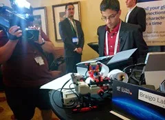
Shubham Banerjee, CEO of the Braille printer maker Braigo Labs, had closed an early round funding with Intel Capital, the company's venture capital arm, last month to develop a prototype of low-cost Braille printer.
But to attend the event, Banerjee had to take the day off from middle school. That’s because he’s just 13 years old — making him, quite possibly, the youngest recipient of venture capital in Silicon Valley history. (He’s definitely the youngest to receive an investment from Intel Capital.)
“I would like all of us to get together and help the visually impaired, because people have been taking advantage of them for a long time,” Banerjee said. “So I would like that to stop.”
By “taking advantage,” Banerjee is referring to the high price of Braille printers today, usually above $2,000. By contrast, Braigo Labs plans to bring its printer to market for less than $500.
Banerjee has invented a new technology that will facilitate this price cut. Patent applications are still pending, so he wouldn’t divulge any of the details. But the technology could also be used to create a dynamic Braille display — something that shows one line of text at a time by pushing small, physical pixels up and down, and which currently costs $6,500, according to Braigo advisor Henry Wedler, who is blind.
Banerjee also figures that volume production will help keep the price low. Currently, Braille printers cost so much because the demand is low, so current manufacturers need to set a high price in order to recoup their costs.
“The truth is that demand is low in the U.S.,” Banerjee told me. But, he added, if you brought the price low enough there would be huge demand outside the U.S.
Banerjee built the version version of his Lego Braille printer for a science fair. He didn’t know anything about Braille beforehand. In fact, he’d asked his parents how blind people read, he said onstage, and they were too busy to answer. “Go Google it,” he said they told him, so he did.
After learning about Braille, he came up with the idea to make a Braille printer. He showed it at his school’s science fair, then later entered it into the Synopsys Science & Technology Championship, where he won first prize, which included a big trophy and a $500 check.
After that, he started getting a lot of attention on his Facebook page. People kept asking him if they could buy one, he said, which led to the idea of creating a company.
Lego was just for the first prototype, by the way: Future versions will be made with more traditional materials.
So how did Intel come to invest in such a young inventor? His father, Niloy, works for Intel — but that’s not exactly how it happened, according to Niloy.
After working with the beta version of Intel Edison (the chip company’s tiny embeddable microprocessor) at a summer camp, Banerjee’s project came to the attention of Intel, which invited him to show off his printer at the Intel Developer Forum. After appearing at IDF, Intel Capital came calling.
Young Banerjee seems composed in front of crowds, which should serve him well. (That’s not surprising, given that Braigo’s website touts coverage on everything from BoingBoing and SlashGear to CNN and NPR.) When asked onstage, in front of 1,000 entrepreneurs, investors, and Intel employees, how he knew that the printer worked even though he doesn’t read Braille, Banerjee answered immediately, “I Googled it.” The crowd laughed.
“I’m happy that I live in Silicon Valley,” Banerjee said. “So many smart people.”
Monday, 3 March 2014
Do U Know? Mobile devices said to consume more energy on storage tasks

Given the always-on mobile infrastructure - background updates, instant messages, email, updates, file sync, logging and more - lots of background storage I/O is happening all the time. And it's eating your device's power budget.
Researchers from Microsoft and the University of California at San Diego benchmarked how Android and Windows RT mobile devices used energy for storing data. They focused on activities that occur with the screen off, since displays are a major power consumer when lit. "Measurements across a set of storage-intensive micro benchmarks show that storage software may consume as much as 200x more energy than storage hardware on an Android phone and a Windows RT tablet," the research team wrote in a paper. "The two biggest energy consumers are encryption and managed language environments."
Results
On Windows RT they found that the OS/CPU/DRAM overhead was between 5 and 200 times the power used by the flash storage itself, depending on how DRAM power use was allocated. File system APIs, the language environment and encryption drove the CPU power consumption during I/O. Full disk encryption - protecting user data - incurred 42 percent of CPU utilization.
On an Android phone, the encryption penalty is even worse: 2.6–5.9x more energy per KB over non-encrypted I/O.
For applications, the team found that on Windows RT, the energy overhead in a managed environment is 12.6–18.3 percent while overhead on Android is between 24.3–102.1 percent. It appears that Android's algorithms are not optimized for application I/O power efficiency.
Sunday, 26 January 2014
Intel Introduces 2 Ultra-Low-Power Mobile Chips

The Haswell rollout has solidified the company's dominance in the computer chip business (including what it claims are record sales of desktop Core i7 CPUs), especially on the mobile side of things. Intel is looking to further its advantage with the release of a new batch of fourth-generation Core processors designed for notebooks.
The nine new mobile Haswell CPUs are a mix of Core i5 and i7 chips that will power performance portables, though a couple are ultra-low-voltage (ULV) processors that can be used in Ultrabooks.The cheapest new one is the i5-4310M at $225 (prices will factor into the cost of a new notebook, as the laptop upgrade market is neglible); its two cores run at 2.7GHz. For about $40 more, the i5-4340M goes to 2.9GHz, while for svelte systems, there's the 2GHz i5-4310U and the 1.5GHz 4360U. Despite the slower clock speed, the 4360U costs more than the other ULV chip because it makes use of Intel's more powerful HD 5000 graphics.
Even though these are new processors, they aren't a quantum leap beyond their predecessors. Because they are clocked about 100MHz higher than the initial Haswell CPUs, that's only about a few percentage points better in performance. But who's going to argue with faster, especially when it's going to be baked into new laptops over the next few months.
Thursday, 23 January 2014
3D graphene-like material promises super electronics

Researchers around the world have looked for ways to take full advantage of its many desirable properties. Now scientists have discovered a material that has a similar electronic structure to graphene but can exist in three dimensions, instead of a flat sheet like graphene, could lead to faster transistors and more compact hard drives.
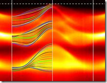
Plot of energy levels of electrons in trisodium bismuthide showing that this bulk material has properties similar to graphene.
The material is called three-dimensional topological Dirac semi-metal (3DTDS) and is a form of the chemical compound sodium bismuthate, Na3Bi.
Researchers led by scientists from Oxford University, Diamond Light Source, Rutherford Appleton Laboratory, Stanford University, and Berkeley Lab's Advanced Light Source, has discovered 3DTDS.
'The 3DTDS we have found has a lot in common with graphene and is likely to be as good or even better in terms of electron mobility – a measure of both how fast and how efficiently an electron can move through a material,' said Dr Yulin Chen of Oxford University's Department of Physics.
'You can think of the electronic structure of the 3DTDS as being rather like that of the graphene – the so called ''Dirac cone'' where electrons collectively act as if they forget their mass – but instead of flowing masslessly within a single sheet of atoms, the electrons in a 3DTDS flow masslessly along all directions in the bulk.'
Moreover, unlike in graphene, electrons on the surface of the 3DTDS remember their 'spin' – a quantum property akin to the orientation of a tiny magnet that can be used to store and read data – so that the magnet information can be directly transferred by the electric current, which could enable faster and more efficient spintronic devices.
'An important property of this new type of material is its magnetoresistance – how its electrical resistance changes when a magnetic field is applied,' said Dr Chen. 'In typical Giant Magnetoresistance Materials (GMR) the resistance changes by a few tens of percent and then saturate but with 3DTDS it changes 100s or 1000s of percent without showing saturation with the external magnetic field. With this much larger effect we could make a hard drive that is higher intensity, higher speed, and lower energy consumption – for example turning a 1 terabyte hard drive into a drive that can store 10 terabytes within the same volume.'
While this particular compound is too unstable to use in devices, the team is testing more stable compounds and looking for ways to tailor them for applications.
Dr Chen said: 'Now that we have proved that this kind of material exists, and that such compounds can have one of the highest electron mobilities of any material so far discovered, the race is on to find more such materials and their applications, as well as other materials with unusual topology in their electronic structure.'
Friday, 3 January 2014
India's fab project fails to attract big chip players

Under the current proposals, Jaypee has tied up with IBM and Tower Jazz and has proposed a facility in Greater Noida with an investment of Rs 26,300 crore, while HSMC has partnered with ST Microelectronics and Silterra and has planned its unit at Prantij near Gandhinagar in Gujarat with an investment of Rs 25,250 crore.
India is trying to create an electronics manufacturing ecosystem to prevent the loss of billions of dollars of foreign exchange in such imports every year. This bill, expected to reach $55 billion (aboutRs 3.4 lakh crore) by 2020 from about $7 billion (Rs 43,600 crore) now, is projected to outstrip oil imports, according to a report commissioned by the industry lobby India Electronics and Semiconductor Association last year.
According to two government officials, the Department of Electronics and Information Technology (DeitY) has received only two new proposals - one by Interactivity Group (supported by a group of IIT alumni) and another by APSTL, an Arizona-headquartered technology firm. Even though an empowered committee set up to evaluate all the proposals is still studying them, an official said it is unlikely something concrete will come out of the two new applications.
With the government's support for setting up the fab firming up at about 40 per cent of the total cost, officials were keen on figuring out if other chipmakers could also be enticed to show interest.
Typically, setting up a chip foundry costs around $4-5 billion (Rs 24,800-31,000 crore). "The idea was, with the incentives firmed up, could we push the fence-sitters off the fence, but that didn't happen," the industry executive said. The deadline to submit initial plans in the fab under a separate call for expressions of interest ran out in November, and there have been no new viable plans submitted other than the two the government had already approved in-principle.
However, a lack of interest the second time around as well underlines the concerns about the feasibility of setting up fab units in the country. Experts argue the long-gestation period and the technology mandates of the government may diminish the usefulness of the projects when they finally come up. The facilities are expected to start production only sometime in 2017.
Thursday, 12 December 2013
Broadcom releases satellite-constellation location IC

The company’s new GNSS SoC is based on its widely deployed architecture that reduces the “time to first fix” (TTFF) and allows smartphones to quickly establish location and rapidly deliver mapping data. The SoC also features a tri-band tuner that enables smartphones to receive signals from all major navigation bands (GPS, GLONASS, QZSS, SBAS, and BeiDou) simultaneously.
The BCM47531 platform is available with Broadcom’s Location Based Services (LBS) technology that delivers satellite assistance data to the device and provides an initial fix time within seconds, instead of the minutes that may be required to receive orbit data from the satellites themselves.
The BCM47531 brings a number of powerful features to the table:
- Simultaneous support of five constellations (GPS, GLONASS, QZSS,SBAS and BeiDou) allows for position calculations based on measurements from any of 88 satellites.
- Broadcom's tri-band tuner brings the ability to receive all navigation bands, GPS (which includes QZSS and SBAS), GLONASS and BeiDou simultaneously to the commercial GNSS market without having to reconfigure and hop between bands.
- Utilizes BeiDou signals for up to 2x improved positioning accuracy.
- Best-in-class Assisted GNSS (AGNSS) data available worldwide from Broadcom's hosted reference network.
- Allows a device to interchangeably use the best signal from any satellite regardless of the constellation, ensuring better accuracy in urban and mountainous environments.
- Features advanced digital signal processing for interference rejection that enables satellite signal search and tracking during LTE transmission.
- Leverages Broadcom's connectivity solutions including Wi-Fi, Bluetooth Smart, Near Field Communications (NFC), Instant Messaging System (IMES) and handset inertial sensor data for best indoor/outdoor location.
Saturday, 28 September 2013
China used more than half of world's ICs in 2012

With an 8.7 percent growth in 2012, China's semiconductor use was 52.5 percent of the total worldwide, said a PwC report titled China's Impact on the Semiconductor Industry - 2013 Update. Semiconductors act as an engine now driving an increasing amount of the technology in people's lives.
The growth in Chinese semiconductor use is a remarkable contrast to the global market for semiconductors, which experienced an overall decline of3 percent in 2012, the report said.
China is expected to continue its domination of semiconductor purchasing in the foreseeable future with its market share possibly reaching 60 percent by 2017,Raman Chitkara, PwC's global technology and semiconductor leader, said in an interview with China Daily.
"One of the major reasons why China has grown so big in semiconductor consumption is that the country isrising to become the world's capital of electronic manufacturing," Chitkara said.
Sunday, 15 September 2013
India Plans To Build 2 Wafer Fabs
 The government of India on Thursday approved "in principle" a plan to construct and equip two wafer fabrication facilities in the country, in a move designed to reduce India's reliance on imported semiconductors. Two consortia will go ahead with the twin fab projects. One is led by STMicroelectronics, an integrated device manufacturer, and the other is spearheaded by Tower Semiconductor, a silicon foundry. These companies will add their names to list of VLSI companies in India and boost the manufacturing capability.
Thursday, 12 September 2013
Cisco’s nPower chips for moving data at 400 Gbps

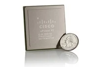
The biggest provider of routing and switching systems has long retained the capability to design specialized processors for its hardware, as well as turn to off-the-shelf chips from commercial suppliers where that makes the most sense. Now Cisco designers have come up with another singular piece of home-grown silicon.
It’s a new product line called the nPower, and Cisco says the chips can pump as much as 400 gigabits of data per second. By contrast, the company’s prior technology could handle 140 gigabits and required more than one chip, Cisco says. The new capacity translates into hundreds of millions of transactions per second.
To what end? Of course, computer and smartphone users will continue to watch more YouTube videos and the like. But Surya Panditi, Cisco’s senior vice president and general manager of engineering, says a key driver for the technology is a coming change in the nature of network traffic.
Wednesday, 4 September 2013
Android Kitkat

Just when all of us thought that Android 5.0 Key Lime Pie would be the next upcoming version of the Android OS, Google has announced that the successor of the Android 4.3 Jelly Bean would be named KitKat (yeah, the brand) and it is Android 4.4, not 5.0 as rumored before.
Sundar Pichai, the Android and Chrome head has confirmed the naming scheme of the next version of Android. Android 4.4 KitKat is named after Neslte's popular candy bar, which is trademarked and licensed by Hershey in the US.
Google also says that "it's our goal with Android KitKat to make an amazing Android experience available for everybody". The bold statement also suggests that Google plans to make use of its next iteration of Android in smart watches, gaming consoles and other electronic gadgets.
Here's the list of past Android versions with the dessert naming scheme:
Android 1.5: Cupcake
Android 1.6: Donut
Android 2.0: Eclair
Android 2.2: Froyo
Android 2.3: Gingerbread
Android 3.0: Honeycomb
Android 4.0: Ice Cream Sandwich
Android 4.1: Jelly Bean
Android 4.2: Jelly Bean
Android 4.3: Jelly Bean
Android 4.4: KitKat
Tuesday, 3 September 2013
Microsoft To Acquire Nokia's Devices And Services

Nokia has seem somewhat of a resurgence lately with a series of high quality smartphones on the Windows Phone platform. Many of the phones such as the Lumia 928, 928 and 1020 with it's 41 megapixel are excellent devices and offer a real choice for anyone wanting to escape the ecosystems of Apple and Android. In fact the majority of users who actually try their Windows Phones quickly find that they enjoy the very different experience they have had with their previous smartphones. The problem for Nokia and Microsoft was getting users to even think about separating from their iPhone or Android device.
According to the companies' press releases, 32,000 people will transfer across Microsoft, including 4,700 people in Finland and 18,300 employees directly involved in product manufacture. If you thought it was only the Windows Phone component of the phone business, you'd be wrong: Microsoft will also take into ownership Nokia's Asha range of feature phones. Patent-wise, Microsoft gets 10-year non-exclusive license to its Finnish partner's library of ideas and "reciprocal rights" to use Microsoft patents within its HERE mapping services. While Microsoft will be able to use the Nokia branding on its products, the Finnish company will now focus on its mapping, infrastructure and advanced tech arms.
In 2011, after writing a memo that said Nokia lacked the in-house technology and needed to jump off a "burning platform", Elop made the controversial decision to use Microsoft's Windows Phone for smartphones, rather than Nokia's own software or Google's (GOOG.O) ubiquitous Android operating system.
The deal will see Microsoft taking full control over Nokia's Smart Devices and Mobile Phones business units, which produce the Lumia family of smartphones and low-cost featurephones respectively. Nokia, meanwhile, retains its telecommunications hardware business Nokia Siemens Networks, Here location-based services arm, and its patent portfolio under the Advanced Technologies division. These patents are to be licensed to Microsoft for at least a ten-year period, the agreement states.
The acquisition will truly allow Microsoft to enter the market in direct competition with its Windows Phone licensees. It's a move that was first telegraphed by the launch of the Surface family, which put the company in direct competition with third part manufacturer's in the Windows 8 and Windows RT tablet markets.
Nokia first started producing phones back in 1996 and for many years they were one of main innovators of smartphones. Of course the release of the iPhone in 2007 and the emergence of Android devices began to strangle Nokia. During the past couple of years Microsoft has provided a kind of life boat to Nokia with their Windows Phones and now it looks like Microsoft has taken over the reins entirely.
Time will tell for both Nokia and Microsoft, but at this very early point I believe it is a good move for both companies and consumers.
Thursday, 8 August 2013
NVIDIA Sets Up New Tech Center Near Detroit

Even with such successes, the automotive industry is still a small part of Nvidia's overall business - but the new technology centre looks to shift that balance. Located in Michigan, a short distance from infamous car-centric Detroit, the centre will concentrate on building technologies specifically for the automotive industry.
Wednesday, 24 July 2013
Motorola touts the power of 8 cores in new phone SoC

-
This is 8-bit microprocessor with 5 instructions. It is based on 8080 architecture. This architecture called SAP for Simple-As-Possible comp...
-
String data type is used for storing strings, the size is dynamic and string data types come with build in methods. If you have ever tried...
-
Q1: What is UVM? What is the advantage of UVM? Ans: UVM (Universal Verification Methodology) is a standardized methodology for verify...
-
1. 8-bit Micro Processor 2. RISC Processor in VLDH 3. Floating Point Unit 4. LFSR - Random Number Generator 5. Versatile Counter 6. ...
-
We would like to write this post for our friends who wants to create a simple FPGA Project with Xilinx ISE. Software Xilinx ISE as a soft...


