Featured post

Top 5 books to refer for a VHDL beginner

VHDL (VHSIC-HDL, Very High-Speed Integrated Circuit Hardware Description Language) is a hardware description language used in electronic des...

Friday, 26 February 2010

Multiplexer

A multiplexer performs the function of selecting the input on any one of 'n' input lines and feeding this input to one output line.


Assume that we have four lines, C0C1C2 and C3, which are to be multiplexed on a single line, Output (f). The four input lines are also known as the Data Inputs. Since there are four inputs, we will need two additional inputs to the multiplexer, known as the Select Inputs, to select which of the C inputs is to appear at the output. Call these select lines A and B.
The gate implementation of a 4-line to 1-line multiplexer is shown below:


Saturday, 6 February 2010

Xilinx Virtex-6 FPGA Family Achieves Full Production Qualification on UMC’s High-Performance 40nm


UMC, a leading global semiconductor foundry, and Xilinx Inc. (XLNX) today announced they have fully qualified the Virtex(R)-6 FPGA family on the foundry's high- performance 40nm logic process. The qualification is the result of the close work between engineering teams from both companies to further enhance yield, reliability and cycle time. The full qualification of the Virtex-6 family signifies the transition to 40nm volume production following UMC's first shipments of the devices in March 2009.
"We highly value the ongoing execution of our long time manufacturing partner UMC," said Xilinx CEOMoshe Gavrielov. "We have collaborated together to deliver several generations of industry leading FPGA families."
"This 40nm achievement follows a long history of successful product family launches with Xilinx," said UMC CEO Dr. Shih-Wei Sun. "Today's production readiness of the 40nm Virtex-6 family underscores our ongoing commitment to Xilinx and our long-term partnership."
Built using third-generation Xilinx ASMBL(TM) architecture, the Virtex-6 FPGA family delivers 15% higher performance and 15% lower power consumption compared to competitive 40nm FPGA offerings. The devices operate on a 1.0v core voltage with an available 0.9v low-power option and are supported by a new generation of development tools delivered by ISE(R) Design Suite 11 and a vast library of IP already available for the market leading 65-nm Virtex-5 FPGA family to ensure productive development and design migration.
"Reaching the production milestone means we have stable and predictable yields that allow us to meet our growing customer demands reliably," said Vincent Tong, Xilinx Senior Vice President, New Product Introductions and Worldwide Quality. "This would not be possible without the joint collaboration with UMC where we used Xilinx's next generation FPGA diagnostic tools along with UMC's rapid info-turn yield learning vehicles to achieve significant yield and quality improvement of 40nm."
Early engagement, design for manufacturing and an effective test vehicle process are also contributing to the successful roll-out of the Virtex-6 family. By building on what they learned from working together closely on previous generations, the Xilinx and UMC engineering teams were able to beat the tape-out to production duration of the Virtex-5 family by a quarter, Tong noted.
"The successful qualification of Virtex-6 is the result of the close teamwork between Xilinx and UMC engineers to address the challenges of 40nm high performance technology," said S.C. Chien, Vice President of Advanced Technology Development at UMC. "UMC dedicated significant engineering talent and resources in our joint effort with Xilinx, such as customizing device specifications to their product specifications, delivering DFM for stable yield, fast info-turn vehicle to enhance quality, and quick diagnosis methodology. We are excited to see that our teamwork has paid off with today's milestone."
UMC's independently developed 45/40nm logic process utilizes sophisticated immersion lithography for its 12 critical layers and incorporates the latest technology advancements such as ultra-shallow junction, embedded silicon- germanium and mobility enhancement techniques, and ultra low-k dielectrics. Currently, several customers have 45/40nm products being manufactured at UMC, with thousands of wafers having already been shipped.
Virtex-6 FPGAs are the programmable silicon foundation for Targeted Design Platforms that deliver integrated software and hardware components to enable designers to focus on innovation as soon as their development cycle begins. The Virtex-6 FPGA family comprises three domain-optimized FPGA platforms that deliver different feature mixes, including DSP slices, memory blocks and serial transceivers supporting up to 11.2Gb/s to best address a variety of customer applications. Currently, six out of nine Virtex-6 family base devices are shipping. All nine are scheduled to be available in production volumes by the end of the second quarter of CY2010.
About UMC
UMC ( UMC, TSE: 2303) is a leading global semiconductor foundry that provides advanced technology and manufacturing services for applications spanning every major sector of the IC industry. UMC's customer-driven foundry solutions allow chip designers to leverage the strength of the company's leading-edge processes, which include production proven 65nm, 45/40nm, mixed signal/RFCMOS, and a wide range of specialty technologies. Production is supported through 10 wafer manufacturing facilities that include two advanced 300mm fabs; Fab 12A in Taiwan and Singapore-based Fab 12i are both in volume production for a variety of customer products. The company employs approximately 12,000 people worldwide and has offices in TaiwanJapanSingaporeEurope, and the United States. UMC can be found on the web athttp://www.umc.com .
About Xilinx
Xilinx is the worldwide leader in complete programmable logic solutions. For more information, visithttp://www.xilinx.com/ .
XILINX, the Xilinx Logo, Virtex, Spartan, ISE and other designated brands included herein are trademarks of Xilinx in the United States and other countries. All other trademarks are the property of their respective owners.

Tuesday, 2 February 2010

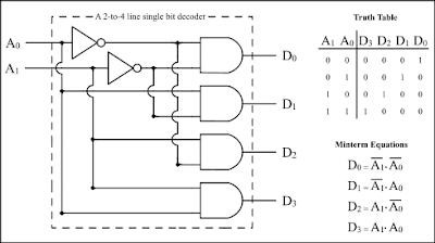
Decoder

Decoder is a multiple input; multiple output logic circuit that converts coded inputs in coded outputs, where input and output codes are different.

Inputs have fewer inputs than output. Below is a simple example of 2-to-4 decoder.


Friday, 18 December 2009

Intel Unveils 32nm Chips

Intel on Thursday said it is in volume production of its next-generation 32-nanometer desktop and laptop chips, with products available for low-end, mainstream and high-end PCs.

A total of 17 new CPUs, along with three new chipsets and seven chips providing Wi-Fi and WiMax support, will be available in computer makers' products early next year, following the International Consumer Electronics Show in January, Intel executives said during a news conference in San Francisco. The new products will be in computers covering 400 separate designs.


All the new products are built using Intel's next-generation 32-nanometer technology, codenamed Westmere, and are based on the Nehalem microarchitecture. The brands are Core i3 for low-end systems, Core i5 for mainstream PCs and Core i7 for the highest end computers used in video editing and playing top-of-the line video games. Intel started shipping 32-nanometer processors this year, but the upcoming products are the first to cover all PC categories.

The Core i7 processors, codenamed Lynnfield for the desktop models and Clarksfield for the laptop versions, are all quad-core processors. The i5 processors are available in quad-core and dual-core models, and the i3 are only dual-core.

All of the dual-core processors have the CPU and graphics processor integrated on a single die, with the memory controller on a separate chip. Previous generations had each of the three components on a separate die. The Core i7 products, which are typically used in systems with a separate graphics card, do not have integrated graphics, which Intel now calls its HD (high-definition) Graphics. Previously, Intel called its graphics technology GMA for graphics media accelerator.

Intel says its latest graphics technology is better than the previous generation because more of the work is done on the hardware versus software. As a result, end users will see smoother, sharper and more colorful playback of Blu-ray video and DVDs. The same is true for picture-in-picture playback, according to Intel.

In addition, Intel graphics support multiple monitors and DisplayPort and Dual HDMI interfaces. The former is used to connect to monitors and home-theater systems and the latter to audio/video devices, such as Blu-ray disc players, set-top boxes and video-game consoles.

The Core i5 and i7 products will all have Intel's Turbo-Boost technology, which ratchets up processing power to meet workload bursts and then lowers it when extra horsepower is no longer needed. The technology also has what Intel calls "power-gating," which will leave idle all cores that aren't needed to accomplish particular tasks. Turbo-Boost technology in general makes processors more efficient in terms of energy use.

Intel plans to release pricing and further details on the new products at CES, which runs from Jan. 7-10 in Las Vegas, Nev.

Intel unveiled its new line the same day researcher IDC released an upbeat report on the PC market. The analyst firm said the overall market in terms of shipments returned to year-over-year growth in the third quarter after three consecutive quarters of decline. Starting next year, IDC says shipments will increase in the low double-digits through 2013.

While facing a brighter outlook for the PC industry, Intel is looking at dark clouds on the legal front. The chipmaker is dealing with increasing pressure from government agencies in and outside the U.S. that accuse the company of anti-competitive behavior. Intel's latest legal headache came this week from the Federal Trade Commission, which used the company, claiming it uses its dominance to stifle competition.


Sunday, 18 October 2009

Sequential Circuits


Sequential logic differs from combinational logic in that the output of the logic device is dependent not only on the present inputs to the device, but also on past inputs; i.e., the output of a sequential logic device depends on its present internal state and the present inputs. This implies that a sequential logic device has some kind of memory of at least part of its ``history'' (i.e., its previous inputs). Below figure shows a generic structure for sequential circuit.


The memory elements are devices capable of storing binary info. The binary info stored in the memory elements at any given time defines the state of the sequential circuit. The input and the present state of the memory element determines the output. Memory elements next state is also a function of external inputs and present state. A sequential circuit is specified by a time sequence of inputs, outputs, and internal states.

There are two types of sequential circuits. Their classification depends on the timing of their signals:

  • Synchronous sequential circuits
  • Asynchronous sequential circuits


  • Asynchronous sequential circuits: This is a system whose outputs depend upon the order in which its input variables change and can be affected at any instant of time.

    Gate-type asynchronous systems are basically combinational circuits with feedback paths. Because of the feedback among logic gates, the system may, at times, become unstable. Consequently they are not often used. Below is an example circuit.


    Synchronous sequential circuits:This type of system uses storage elements called flip-flops that are employed to change their binary value only at discrete instants of time. Synchronous sequential circuits use logic gates and flip-flop storage devices. Sequential circuits have a clock signal as one of their inputs. All state transitions in such circuits occur only when the clock value is either 0 or 1 or happen at the rising or falling edges of the clock depending on the type of memory elements used in the circuit. Synchronization is achieved by a timing device called a clock pulse generator. Clock pulses are distributed throughout the system in such a way that the flip-flops are affected only with the arrival of the synchronization pulse. Synchronous sequential circuits that use clock pulses in the inputs are called clocked-sequential circuits. They are stable and their timing can easily be broken down into independent discrete steps, each of which is considered separately.
    Below figure shows example circuit:


    A clock signal is a periodic square wave that indefinitely switches from 0 to 1 and from 1 to 0 at fixed intervals. Clock cycle time or clock period: the time interval between two consecutive rising or falling edges of the clock.

    Thursday, 15 October 2009

    Combinational circuits


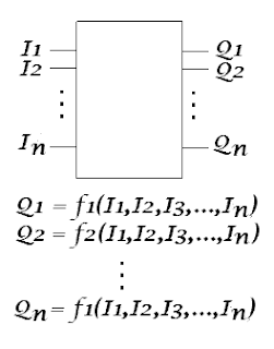
    Combinatorial Circuits are circuits which can be considered to have the following generic structure.

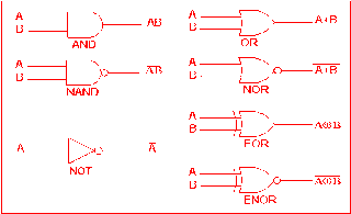
    Whenever the same set of inputs is fed in to a combinatorial circuit, the same outputs will be generated. Such circuits are said to be stateless. Some simple combinational logic elements that we have seen in previous sections are "Gates".

    Below figure shows the basic gates that are used to build a combinational circuit.

    Tuesday, 13 October 2009

    PCI Express: "A Layered Architecture"

    PCI Express is a layered protocol, consisting of a transaction layer, a data link layer, and a physical layer. The Data Link Layer is subdivided to include a media access control (MAC) sublayer. The Physical Layer is subdivided into logical and electrical sublayers. The Physical logical-sublayer contains a physical coding sublayer (PCS). (Terms borrowed from the IEEE 802 model of networking protocol.)

    PCI Express Layered Architecture

    Configuration/Operating System Layer —Leverages the standard mechanisms defined in the PCI Plug-and-Play specification for device initialization, enumeration, and configuration. This layer communicates with the software layer by initiating a data transfer between peripherals or receiving data from an attached peripheral. PCI Express is designed to be compatible with existing operating systems, but future operating system support is required for many of the technology’s advanced features.

    Software Layer —Generates read and write requests to peripheral devices. PCI Express maintains initialization and runtime software compatibility with PCI. Like PCI, the PCI Express initialization model allows the operating system to discover add-in hardware devices and allocate system resources. PCI Express retains the PCI configuration space and the programmability of I/O devices. In fact, all operating systems will boot without modification on a PCI Express system. The PCI runtime software model is also preserved, enabling existing software to execute unchanged.

    Transaction Layer —Transports read and write requests from the software layer to the link layer using a packet-based protocol, and matches response packets to the original software requests. The transaction layer supports 32-bit and extended 64-bit memory addressing. It also supports PCI memory, I/O, and configuration address spaces, as well as a new message space for in-band messages such as interrupts and resets. This message space eliminates the need for numerous PCI and PCI-X sideband signals.

    Link Layer —Adds sequencing and error detection cyclic redundancy codes (CRCs) to the data packets to create a reliable data transfer mechanism between the system chip set and the I/O controller.

    Physical Layer —Implements the dual simplex PCI Express channels. Implementations are flexible and various technologies and frequencies may be used. In this way, initial silicon technology can be replaced easily with future implementations that are backward compatible. For example, fiber-optic technology might be used to increase the data transfer rate.

    Mechanical Layer —Defines various form factors for peripheral devices.