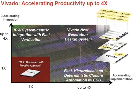
Xilinx Inc. has announced the Vivado Design Suite. It enables an IP and system centric next generation design environment. Especially meant for the next decade of ‘All-Programmable’ devices, it also accelerates the integration and implementation up to 4X. And, why now? That’s because the all-programmable devices enable programmable systems ‘integration.

There are implementation bottlenecks as well, such as hierarchical chip planning, multi-domain and multi-die physical optimization, predictable ‘design’ vs. ‘timing’ closure, and late ECOs and rippling effect of changes.
Vivado accelerates productivity up to 4X. The design suite elements include an integrated design environment, has a shared scalable data model, is scalable to 100 million gates, and debug and analysis. It shares design information between implementation steps that ensures fast convergence and timing closure. This enables highly efficient memory utilization. Also, it is scalable to future families, that are greater than 10 million logic cells (100 million gates) and enables cross-probing across the entire design.
Vivado also enables packaging designs into system-level IP for re-use. You can share IP within your team, project or company. Any 3rd party IP is delivered with a common look and feel. You can re-use IP at any point in the implementation process. The IP can be source, placed, or placed and routed.


No comments:
Post a Comment
Please provide valuable comments and suggestions for our motivation. Feel free to write down any query if you have regarding this post.