Featured post

Top 5 books to refer for a VHDL beginner

VHDL (VHSIC-HDL, Very High-Speed Integrated Circuit Hardware Description Language) is a hardware description language used in electronic des...

Showing posts with label Xilinx. Show all posts

Wednesday, 17 April 2013

Xilinx enables C programmable FPGAs

Vivado_xilinx The Vivado Design Suite 2013.1 includes a new IP-centric design environment designed to accelerate system integration, and a set of libraries to accelerate C/C++ system-level design and high-level synthesis (HLS). The update provides a workflow that does not dictate how a design team works.

Users of Vivado HLS can access video processing functions integrated into an OpenCV environment for embedded vision running on the dual-core ARM processing system.

It delivers, says Xilinx, up to a 100X performance improvement of existing C/C++ algorithms through hardware acceleration.

Read more…

Get free daily email updates!

Follow us!

Thursday, 21 February 2013

How to read an NGC netlist file

For the occasions that you find yourself with a netlist file and you don’t know where it came from or what version it is, etc. this post is about how you can interpret the netlist file (ie. convert it into something readable).

Today I found myself with two netlists and I needed to know if they were the same. Yes of course you can try comparing the two files with a program such as Beyond Compare, but if the netlists were compiled on separate dates, you will have trouble recognizing this from the raw binary data. The best thing to do in this case is to convert the netlists to EDIF files, a readable, text file version of the netlist. Another option is to convert the netlists into VHDL or Verilog code. Here is how you can do this:

To convert a netlist (.ngc) to an EDIF file (.edf)

  1. Get a command window open by typing “cmd” in the Start->Run menu option in Windows. If you use Linux, open up a terminal window.
  2. Use the “cd” command to move to the folder in which you keep your netlist.
  3. Type “ngc2edif infilename.ngc outfilename.edf” where infilename and outfilename correspond to the input and output filenames respectively.
  4. Open the .edf file with any text editor to view the netlist.

To reverse engineer a netlist with ISE versions older than 6.1i

  1. Convert the netlist to an EDIF file using the above instructions.
  2. Type “edif2ngd filename.edf filename.ngd” to convert the EDIF file into an NGD file (Xilinx Native Generic Database file).
  3. To convert the netlist into VHDL type “ngd2vhdl filename.ngd filename.vhd“.
  4. To convert the netlist into Verilog type “ngd2ver filename.ngd filename.v“.

To reverse engineer a netlist with ISE versions 6.1i and up

  1. To convert the netlist into VHDL type “netgen -ofmt vhdl filename.ngc“. Netgen will create a filename.vhd file.
  2. To convert the netlist into Verilog type “netgen -ofmt verilog filename.ngc“. Netgen will create a filename.v file.

Now you should have all the tools you need to read an NGC netlist file.

Get free daily email updates!

Follow us!

Wednesday, 23 January 2013

IHS iSuppli: IC inventories hit record levels in Q3

hip inventories reached record highs near the end of 2012, and according to IHS iSuppli, semiconductor revenue will decline in Q1, prompting new concerns about the state of the market.

Overall semiconductor revenue is expected to slide three percent between January and March 2013, on top of a 0.7 percent decline in Q4 2012. What's more, inventory reached record levels in Q3 2012, amounting to 49.3 percent of revenue, more than at any point since Q1 2006. IHS iSuppli believes the uncomfortably high level of inventory points to the failure of key demand drivers to materialize.

The PC market remains slow and hopes of a Windows 8 renaissance have turned into a nightmare. Bellwether Intel saw its revenue drop three percent in Q4, with profit tumbling 27 percent, and the trend is set to continue. AMD is expected to announce its earnings Tuesday afternoon and more gloom is expected across the board. The only bright spot in an otherwise weak market is TSMC, which quickly rebounded after posting the lowest revenues in two years a year ago. TSMC now expects to see huge demand for 28nm products in 2013 and many observers point to a possible deal with Apple.

In addition, TSMC plans to invest $9 billion in capital expenditure in 2013, and it will likely spend even more in 2014, as it moves to ramp up 20nm production. However, Intel's plans to increase capital spending to $13 billion, up $2 billion over 2012 levels, have not been welcomed by analysts and investors. Unlike TSMC, Intel is not investing to increase capacity in the short term, it is making a strategic bet on 450mm wafer technology, which promises to deliver significantly cheaper chips compared to existing 300mm wafers. However, 450mm plants are still years away.

TSMC's apparent success has a lot to do with high demand for Smartphone's and tablets, which are slowly eating into the traditional PC market. Semiconductor shipments for the wireless segment were expected to climb around four percent in 2012 and positive trends were visible in analog, logic and NAND components. However, the mobile boom can't last forever, and we are already hearing talk of "Smartphone fatigue" and "peak Apple".

IHS iSuppli estimates the first quarter of 2013 will see growth in industrial and automotive electronics and other semiconductor markets will eventually overcome the seasonal decline, so a rebound is expected in the second and third quarters.

Semiconductor revenue could grow by four percent in the second, and nine percent in the third quarter. However, the assumptions are based on a wider economic recovery, which is anything but certain at this point. If demand evaporates, semiconductor suppliers could find themselves hit by an oversupply situation, leading to more inventory write-downs throughout the year.

Get free daily email updates!

Follow us!

Tuesday, 15 January 2013

SEMI Industry spending $32.4B this year on IC gear

ics Fab equipment spending saw a drastic dip in 2H12 and 1Q13 is expected to be even lower, says SEMI, which reckons that the projected number of facilities equipping will drop from 212 in 2012 to 182 in 2013.

Spending on fab equipment for System LSI is expected to drop in 2013. Spending for Flash declined rapidly in 2H12 (by over 40 %) but is expected to pick up by 2H13. The foundry sector is expected to increase spending in 2013, led by major player TSMC, as well as Samsung and Global foundries.

Fab construction:
While fab construction spending slowed in 2012, at -15%,  SEMI  projects an increase of 3.7 % in 2013 (from $5.6bn in 2012 to $5.8bn  in 2013).

The report tracks 34 fab construction projects for 2013 (down from 51 in 2012).  An additional 10 new construction projects with various probabilities may start in 2013. The largest increase for construction spending in 2013 is expected to be for dedicated foundries and Flash related facilities.

Many device manufacturers are hesitating to add capacity due to declining average selling prices and high inventories.

However SEMI reckons flash capacity will grow 6%  by mid-2013, with nearly 6 % growth, adding over 70,000wpm.

SEMI also foresees a rapid increase of installed capacity for new technology nodes, not only for 28nm but also from 24nm to 18nm and first ramps for 17nm to 13nm in 2013.

SEMI cautiously forecasts  fab equipment spending in 2013 to range from minus 5 to plus 3.

Get free daily email updates!

Follow us!

Sunday, 13 January 2013

Full Speed Ahead For FPGA

droppedImageIn the world of high-frequency trading, where speed matters most, technology that can gain a crucial split-second advantage over a rival is valued above all others.

And in what could be the next phase of HFT, firms are looking more and more to hardware solutions, such as field-programmable gate array (FPGA), as it can offer speed gains on the current software used by HFT firms.

FPGA technology, which allows for an integrated circuit to be designed or configured after manufacturing, has been around for decades but has only been on the radar of HFT firms for a couple of years. But new solutions are beginning to pop up that may eventually see FPGA become more viable and be the latest must-have tool in the high-speed arms race.

For instance, a risk calculation that can take 30 microseconds to perform by a software-based algorithm takes just three microseconds with FPGA.

Current HFT platforms are typically implemented using software on computers with high-performance network adapters. However, the downside of FPGA is that it is generally complicated and time consuming to set up, as well as to re-program, as the programmer has to translate an algorithm into the design of an electronic circuit and describe that design in specialized hardware description language.

The programming space on FPGA is also limited, so programs can’t be too big currently. Although, some tasks such as ‘circuit breakers’ are an ideal current use for FPGA technology.

It is the drawbacks, as well as the costs involved, that are, at present, are holding back trading firms from taking up FPGA in greater numbers. However, because of the speed gains that it offers, much resources are being poured into FPGA in a bid to make the technology more accessible—and some technology firms are now beginning to claim significant speed savings with their products.

Cheetah Solutions, a provider of hardware solutions for financial trading, is one firm that says it can now offer reconfigurable FPGA systems to trading firms. It says its Cheetah Framework provides building blocks which can be configured in real time by a host server and an algorithm can execute entirely in an FPGA-enabled network card with the server software taking only a supervisory role by monitoring the algo’s performance and adapting the hardware algo on the go.

“True low latency will only be achieved through total hardware solutions which guarantee deterministic low latency,” said Peter Fall, chief executive of Cheetah Solutions. “But if the market moves, you want to be able to tweak an algorithm or change it completely to take advantage of current conditions. Traditional FPGA programming may take weeks to make even a simple change whereas Cheetah Framework provides on-the-fly reconfigurability.”

Another technology firm to claim that it can make automated trading strategies even faster and more efficient is U.K.-based Celoxica, which recently debuted its new futures trading platform, based on FPGA technology, which involves a circuit on one small chip that can be programmed by the customer.

Celoxica says the platform is designed to accelerate the flow of market data into trading algorithms to make trading faster. It covers multiple trading strategies and asset classes including fixed income, commodities and foreign exchange.

“For futures trading, processing speed, determinism and throughput continue to play a crucial role in the success of principle trading firms and hedge funds trading on the global futures markets,” said Jean Marc Bouleier, chairman and chief executive at Celoxica. “Our clients and partners can increase focus on their trading strategies for CME, ICE, CFE, Liffe US, Liffe and Eurex.”

While last August, Fixnetix, a U.K. trading technology firm, said that it had signed up a handful of top-tier brokers to use its FPGA hardware chip, which executes deals, compliance and risk checks, suggesting that this niche technology is picking up speed rapidly.

Wednesday, 5 December 2012

Creating a simple FPGA Project with Xilinx ISE

Xilinx Virtex5 LX300 FPGA chip on the board

We would like to write this post for our friends who wants to create a simple FPGA Project with Xilinx ISE. 

Software

Xilinx ISE as a software package containing a graphical IDE, design entry tools, a simulator, a synthesizer (XST) and implementation tools. Limited version of Xilinx ISE (WebPack) can be downloaded for free from the Xilinx website.

It is not mandatory to use Xilinx software for all tasks (for example, synthesis can be done with Synplify, simulation - with Modelsim etc.), but it is the easier option to start off.

The information in this article applies to Xilinx ISE version 9.2.03i, but other versions (since 8.x) shouldn't be very different. If your version is older than 8.x, you'd better upgrade.

Creating a project

To create a project, start a Project Navigator and select File->New Project. You will be asked for project name and folder. Leave "top-level source type" as HDL.

Now we should choose a target device (we will use a Spartan-3A xc3s50a device as an example) as well as set up some other options:

A dialog of creating project in Xilinx ISE

The Project Navigator window contains a sidebar, which is on the left side by default. The upper part of this sidebar lists all project files, and the lower part lists tasks that are applicable for the file selected in the upper part.

Design Entry

Now, let's add a new source file to our project. We'll start from a simple 8-bit counter, which adds 1 to its value every clock cycle. This counter will have the following ports:

  • CLK - input clock signal;
  • CLR - input asynchronous clear signal (set counter value to 0);
  • DOUT - output counter value (8-bit bus).

We'll define our counter as a VHDL module. VHDL language will be covered in more details in further chapters.

To create a new source file, choose "Create New Source" task and select "VHDL module" source type. The name of our module will becounter.vhd. Then you will be asked which module to associate the testbench with; choose counter.

A dialog of creating a new source file in Xilinx ISE

Let's write the following code in counter.vhd:

library IEEE;
use IEEE.STD_LOGIC_1164.ALL;
use IEEE.STD_LOGIC_ARITH.ALL;
use IEEE.STD_LOGIC_UNSIGNED.ALL;

entity counter is
    Port ( CLK : in  STD_LOGIC;
           CLR : in  STD_LOGIC;
           DOUT : out  STD_LOGIC_VECTOR (7 downto 0));
end counter;

architecture Behavioral of counter is

signal val: std_logic_vector(7 downto 0);

begin

process (CLK,CLR) is
begin
    if CLR='1' then
        val<="00000000";
    elsif rising_edge(CLK) then
        val<=val+1;
    end if;
end process;

DOUT<=val;

end Behavioral;

ISE inserted library and ports declarations automatically, we only need to write an essential part of VHDL description (inside thearchitecture block).

To check VHDL syntax, select "Synthesize - XST => Check Syntax" task for our module.

Simulation

In order to check that our code works as intended, we need to define input signals and check that output signals are correct. It can be done by creating a testbench.

To create a testbench for our counter, select "Create New Source" task, choose "VHDL Test Bench" module type and name it, for instance, counter_tb.vhd.

VHDL test bench is written in VHDL, just like a hardware device description. The difference is that a testbench can utilize some additional language constructs that aren't synthesizable and therefore cannot be used in real hardware (for example wait statements for delay definition).

In order for testbench file to be visible, choose "Behavioral Simulation" in the combobox in the upper part of the sidebar.

ISE automatically generates most of the testbench code, we need only to add our "stimulus":

LIBRARY ieee;
USE ieee.std_logic_1164.ALL;
USE ieee.std_logic_unsigned.all;
USE ieee.numeric_std.ALL;

ENTITY counter_tb_vhd IS
END counter_tb_vhd;

ARCHITECTURE behavior OF counter_tb_vhd IS

    -- Component Declaration for the Unit Under Test (UUT)
    COMPONENT counter
    PORT(
        CLK : IN std_logic;
        CLR : IN std_logic;         
        DOUT : OUT std_logic_vector(7 downto 0)
        );
    END COMPONENT;

    --Inputs
    SIGNAL CLK :  std_logic := '0';
    SIGNAL CLR :  std_logic := '0';

    --Outputs
    SIGNAL DOUT :  std_logic_vector(7 downto 0);

BEGIN

    -- Instantiate the Unit Under Test (UUT)
    uut: counter PORT MAP(
        CLK => CLK,
        CLR => CLR,
        DOUT => DOUT
    );
    -- Clock generation   
    process is
    begin
        CLK<='1';
        wait for 5 ns;
        CLK<='0';
        wait for 5 ns;
    end process;

    tb : PROCESS
    BEGIN

        CLR<='1';
        wait for 100 ns;

        CLR<='0';

        wait; -- will wait forever
    END PROCESS;

END;

We have added the clock generation process (which generates 100MHz frequency clock) and reset stimulus.

Now select a test bench source file and apply "Xilinx ISE Simulator => Simulate Behavioral Model" task. We should get something like this:

Xilinx ISE Simulator window

It can be seen that our counter works properly.

Synthesis

The next step is to convert our VHDL code into a gate-level netlist (represented in the terms of the UNISIM component library, which contains basic primitives). This process is called "synthesis". By default Xilinx ISE uses built-in synthesizer XST (Xilinx Synthesis Technology).

In order to run synthesis, one should select "Synthesis/Implementation" in the combobox in the upper part of the sidebar, select a top-level module and apply a "Synthesize - XST" task. If the code is correct, there shouldn't be any pproblems during the synthesis.

Synthesizer report contains many useful information. There is a maximum frequency estimate in the "timing summary" chapter. One should also pay attention to warnings since they can indicate hidden problems.

After a successful synthesis one can run "View RTL Schematic" task (RTL stands for register transfer level) to view a gate-level schematic produced by a synthesizer:

RTL schematic view in Xilinx ISE

Notice that an RTL schematic in question contains only one primitive: a counter, which is directly an element from the UNISIM library.

Synthesizer output is stored in NGC format.

Implementation
Implementation design flow
  1. Translate - convert NGC netlist (represented in the terms of the UNISIM library) to NGD netlist (represented in the terms of the SIMPRIM library). The difference between these libraries is that UNISIM is intended for behavioral simulation, and SIMPRIM is a physically-oriented library (containing information about delays etc.) This conversion is performed by the program NGDBUILD and is rather straightforward. The main reason for it to be included is to convert netlist generated by different design entry methods (e.g. schematic entry, different synthesizers etc.) into one unified format.
  2. Map is a process of mapping the NGD netlist onto the specific resources of the particular device (logic cells, RAM modules, etc.) This operation is performed by the MAP program with resutls being stored in NCD format. For Virtex-5 MAP also does placement (see below).
  3. Place and route - as can be inferred from its name, this stage is responsible for the layout. It performs placement (logic resources distribution) and routing (connectivity resources distribution). Place and route is performed by a PAR program. For Virtex-5 devices, though, placement is performed by MAP program (and routing still by PAR program). The output of PAR is stored, again, in NCD format.
Implementation Constraints

Constraints are very important during the implementation. They define pin assignments, clocking requirements and other parameters influencing implementation. Constraints are stored in UCF format (user constraints file).

In order to add constraints one need to add a new source (using "Create New Source" task) and choose "Implementation constraints file" source type. UCF file is a text file that can be directly edited by a user, however, simple consraints can be defined with graphical interface.

When a constraints file is selected in the upper part of the sidebar, the specific tasks become available. These include "Create Timing Constraints" and "Assign Package Pins".

For example, if we specify a frequency requirement on CLK as 100 MHz, the corresponding section of the constraints file will be:

NET "CLK" TNM_NET = CLK;
TIMESPEC TS_CLK = PERIOD "CLK" 100 MHz;

When timing requirements are specified in the constraints file, the implementation tools will strive to meet them (and report an error in the case it can't be met).

Package pins constraints must also be set (according to the board layout).

MAP program converts UCF constraints to the PCF format which is later used by PAR.

There are also synthesis constraints stored in XCF files. They are used rarely and shouldn't be confused with implementation constraints.

Programming file generation

After placement and routing, a file should be generated that will be loaded into the FPGA device to program it. This task is performed by a BITGEN program.

The programming file has .bit extension.

The programming file is loaded to the FPGA using iMPACT.

Get free daily email updates!

Follow us!

Wednesday, 28 November 2012

Customize the ModelSim Wave View in the Xilinx ISE Simulation

When ModelSim is automatically lunched within the ISE environment it  just displays the top entity level signals in the Wave View window. However, to either facilitate debugging tasks or check specific behavior of lower level components most of the time internal signals also need to be displayed in the Wave View window of ModelSim. Moreover, coloring, ordering and grouping signals  is especially useful in complex designs. Hence, having one or several custom views and invoking them automatically will help the verification job.

Scripts files (.do) created in ISE

When ModelSim is launched from the Xilinx ISE, Project Navigator automatically creates a .do script file that contains all of the necessary commands to compile the .vhd  source  files, load, start  and run the
simulation in ModelSim.
The .do script file created by Project Navigator has different extensions based on the type of simulation launched. For instance, for a Behavioral (functional) Simulation these are the three files created:

<TestBenchName>.fdo           ModelSim commands for behavioral simulation
<TestBenchName>.udo           ModelSim user commands
<TestBenchName_wave>.fdo  ModelSim Wave window format commands for behavioral simulation

A detail of the ModelSim commands in a <TestBenchName>.fdo script file created by Project Navigator, when running a Behavioral Simulation, is described below:

FIG1 The <TestBenchName>.fdo script file is regenerated each time a behavioral simulation is launched. Therefore, any modification done in this file will be automatically overwriting. Still, in this script file there is a command line, do{<TestBenchName_wave>.fdo}, that invokes the <TestBenchName_wave>.fdo script file. This script file never is neither modified nor overwritten by Project Navigator. Hence, the best file that can be used to customize the Wave window format in the ModelSim environment is the <TestBenchName_wave>.fdo script file. By default, this file has the following structure:

imageThe ‘add wave *’ command means that, by default, all the top level entity signals will be displayed in the Wave view of ModelSim. Likewise, when running simulation after translating, mapping or PAR processes, similar script files are created. A detail of the script files created in each process is showed below:

Simulation Post-translate
<TestBenchName>.ndo            ModelSim commands for post-translate simulation
<TestBenchName>.udo            ModelSim user commands
<TestBenchName_wave>.ndo  ModelSim waves format commands for post-translate simulation

Simulation Post-Map Process
<TestBenchName>.mdo ModelSim commands for post-map simulation
<TestBenchName>.udo ModelSim user commands
<TestBenchName_wave>.mdo ModelSim waves format commands for post-map simulation

Simulation Post-PAR
<TestBenchName>.tdo ModelSim commands for post-par simulation
<TestBenchName>.udo ModelSim user commands
<TestBenchName_wave>.tdo ModelSim waves format commands for post-par simulation

In general, the script file <TestBenchName_wave>.*do will be the file to be modified to customize the Wave window in the ModelSim environment in any of the different simulation cases. As it was detailed above, the “add wave *” command states to display just the top level entity signals. However; to facilitate debugging tasks most of the time internal signals also need to be displayed in the Wave window. Moreover, coloring, ordering and grouping the signals in the Wave window is especially useful in complex designs.

Customization Process

The process to customize the Wave window in ModelSim when running the simulation flow in Xilinx ISE environment is detailed below:

1) Create a new ISE project or just open one already created. Write your VHDL code, create your test bench and execute either the functional, post-translate, post-map or post-par simulation of your design, which will open ModelSim simulation tool.

2) Within the Wave window, ModelSim offers several methods to customize the view.

    • Adding internal signals: in the Instance view of ModelSim (left most pane) you can find the test bench name and underneath it, you can see the instance name of the entity under test. The instance name is actually the label used in the instantiation of the top level entity in the test bench. Click over the ‘+’ symbol to be able to see all the unit components of the top level entity. Then, select the unit that holds the signals you want to add to the Wave window by single click over the unit’s name. After that, on the Objects window (usually the window in the middle) the name of the signals of the selected unit will be displayed. Select the signal you want to add to the Wave window by single click over it, then drag and drop the signal into the Wave window. You can repeat this process and add as many signals as needed. Once a signal is added to the Wave window, you can move it up or down as explained below.
    • Moving signals: it is also possible to move either up or down the signals displayed in the Wave window to facilitate reading the waveforms. For instance, you can place all the input signals on the top of all the other signals, then the control signals in the middle and the output signals at the bottom. To move up or down the signals in the Wave window, select the signal you want to move (single right-mouse click over the signal). Then, drag the signal up or down, by keeping the right-mouse button pressed and moving the mouse up or down, and drop the signal, release the mouse button, wherever you like.
    • Adding dividers: signal dividers can be added in the Wave window to label the signals grouped with a specific purpose. For instance, you can add dividers labeled Input Signals, Control Signals, Rx Signals, Memory Read, Clocks, and such. To add a divider select the signal over which you want the divider. Then, right-mouse click and select ‘Insert Divider’ from the down menu. The divider dialog window will come up. You can add a name describing the function of the signals that will be under the divider. You can also set the Divider Height, though this is not usually changed.
    • Coloring the waveform: for some specific purposes, for instance for a quick waveform reference among hundreds of waveforms, it is advantageous to change the color of a specific waveform as well as the color of signal name. Highlight (select) the signal that you want to change the waveform color, then right-mouse click and select Properties, the Wave Properties window should come up. In the View tab, you will find the Wave Color and Name Color selections. To change the default colors, click on the Colors button and select the desired color. When finished, click on Apply.

3) Once you are done adding signal, dividers and changing colors, it is then necessary to save this new customized Wave window format to be able to use it again:

    • Be sure to select (highlight) the Wave window among the other ModelSim views.
    • Go to File -> Save Format. Then, click OK in the Save Format dialog window to save the new wave format in the default directory (ISE project directory) or in the directory you would like by browsing to it. The default name is wave.do. In case you are planning to have a customized wave view for the different simulations (like functional, post-map, post-PAR), change the default wave.do name to something like wave_f.do for functional, wave_m.do for mapping and so on for the other type of simulation.

4) Go back to the ISE Project Manager window.

5) There are a couple of options to load automatically the saved wave.do file (item 3.b) when running a simulation from Project Navigator. As it was explained before, the easiest way is to modify the <TestBenchName_wave.fdo> file. Hence, open to edit the <TestBenchName_wave.fdo> file that resides in the ISE Project Directory. Remove or comment out (by using the # character) the command line “add wave *” and then add a new command line that will invoke the customized waveform; by writing “do wave.do” (or whatever name you use when saving the Wave window format). If you have saved the wave.do file in a directory different than the ISE Project Directory, you will need to write the complete path where the file wave.do resides. Below, there are two examples of how the <TestBenchName_wave.fdo> file would look like, one for a complete directory path, and the other with a relative path:

image

image

Once finishing with the modifications, save the customized <TestBenchName_wave.fdo> file.

6) From now on for every behavioral simulation to be executed, Project Navigator will use the custom wave.do waveform format when launching ModelSim.

Even though it has been explained the process to customize the behavioral simulation, similar steps have to be followed, for instance, for customizing the post-place and route simulation. The file to be changed in this case is the <TestBenchName_wave>.tdo (as it was explained before) and just follows all the steps detailed above for the behavioral simulation.

More on Customization
Besides of modifying the <TestBenchName_wave.fdo> file for customizing the Wave window format, another ModelSim commands can also be added with other purposes. For instance, one useful command for designs with a large amount of internal signals is the following: log –r /*

This command will log all the data objects in the design. For example, if after running the simulation you find out you would like to see an internal signal not currently displayed in the Wave view, you just need to select the signal you want to add, drag and drop it in the Wave view. Then, its respective waveform will immediately be displayed.

Without the log command, if that particular internal signal is not in the list of signals in the wave.do script, it is not logged; therefore no waveform will be displayed for that signal. In this case, it will be necessary to add the signal to the Wave window, save the wave.do again and then rerun the simulation.

The drawback of the log command is that it could make the simulation much slower since it needs to log all the signals of the design. One point to keep in mind is the fact that internal signals after PAR usually do not keep the same name as before the PAR. This means that the wave.do saved for functional simulation, may or may not be able to display all the internal signals when doing a post-PAR simulation.

One solution for this problem is to create another customized wave.do for the post-PAR simulation naming it something like wave_par.do. Then, change the <TestBenchName_wave.tdo> file as explained in point 5 above. Another helpful point to know is the fact that it is possible to rerun the simulation without closing ModelSim, avoiding returning to Project Navigator.

For instance, if you find an error when running the simulation in one of the .vhd source files, you can edit the VHDL file, still keeping open ModelSim (even you can use ModelSim text editor), save the modifications of the VHDL file and rerun the simulation by typing do {TestBenchName.fdo} and pressing enter in the transcript window (bottom window) of ModelSim. You can also use the up-arrow key in the transcript window to go through all the executed commands until you find the do {TestBenchName.fdo} command, and then just press enter to execute it.

Get free daily email updates!

Follow us!

Thursday, 6 September 2012

Choosing FPGA or DSP for your Application


FPGA or DSP - The Two Solutions

The DSP is a specialised microprocessor - typically programmed in C, perhaps with assembly code for performance. It is well suited to extremely complex maths-intensive tasks, with conditional processing. It is limited in performance by the clock rate, and the number of useful operations it can do per clock. As an example, a TMS320C6201 has two multipliers and a 200MHz clock – so can achieve 400M multiplies per second.

In contrast, an FPGA is an uncommitted "sea of gates". The device is programmed by connecting the gates together to form multipliers, registers, adders and so forth. Using the Xilinx Core Generator this can be done at a block-diagram level. Many blocks can be very high level – ranging from a single gate to an FIR or FFT. Their performance is limited by the number of gates they have and the clock rate. Recent FPGAs have included Multipliers especially for performing DSP tasks more efficiently. – For example, a 1M-gate Virtex-II™ device has 40 multipliers that can operate at more than 100MHz. In comparison with the DSP this gives 4000M multiplies per second.


Where They Excel


When sample rates grow above a few Mhz, a DSP has to work very hard to transfer the data without any loss. This is because the processor must use shared resources like memory busses, or even the processor core which can be prevented from taking interrupts for some time. An FPGA on the other hand dedicates logic for receiving the data, so can maintain high rates of I/O.

A DSP is optimised for use of external memory, so a large data set can be used in the processing. FPGAs have a limited amount of internal storage so need to operate on smaller data sets. However FPGA modules with external memory can be used to eliminate this restriction.

A DSP is designed to offer simple re-use of the processing units, for example a multiplier used for calculating an FIR can be re-used by another routine that calculates FFTs. This is much more difficult to achieve in an FPGA, but in general there will be more multipliers available in the FPGA. 

If a major context switch is required, the DSP can implement this by branching to a new part of the program. In contrast, an FPGA needs to build dedicated resources for each configuration. If the configurations are small, then several can exist in the FPGA at the same time. Larger configurations mean the FPGA needs to be reconfigured – a process which can take some time.

The DSP can take a standard C program and run it. This C code can have a high level of branching and decision making – for example, the protocol stacks of communications systems. This is difficult to implement within an FPGA.

Most signal processing systems start life as a block diagram of some sort. Actually translating the block diagram to the FPGA may well be simpler than converting it to C code for the DSP.

Making a Choice

There are a number of elements to the design of most signal processing systems, not least the expertise and background of the engineers working on the project. These all have an impact on the best choice of implementation. In addition, consider the resources available – in many cases, I/O modules have FPGAs on board. Using these with a DSP processor may provide an ideal split.


As a rough guideline, try answering these questions:

  1. What is the sampling rate of this part of the system? If it is more than a few MHz, FPGA is the natural choice.
  2. Is your system already coded in C? If so, a DSP may implement it directly. It may not be the highest performance solution, but it will be quick to develop.
  3. What is the data rate of the system? If it is more than perhaps 20-30Mbyte/second, then FPGA will handle it better.
  4. How many conditional operations are there? If there are none, FPGA is perfect. If there are many, a software implementation may be better.
  5. Does your system use floating point? If so, this is a factor in favour of the programmable DSP. None of the Xilinx cores support floating point today, although you can construct your own.
  6. Are libraries available for what you want to do? Both DSP & FPGA offer libraries for basic building blocks like FIRs or FFTs. However, more complex components may not be available, and this could sway your decision to one approach or the other.

In reality, most systems are made up of many blocks. Some of those blocks are best implemented in FPGA, others in DSP. Lower sampling rates and increased complexity suit the DSP approach; higher sampling rates, especially combined with rigid, repetitive tasks, suit the FPGA.


Some Examples

Here are a few examples of signal processing blocks, along with how we would implement them:

  1. First decimation filter in a digital wireless receiver. Typically, this is a CIC filter, operating at a sample rate of 50-100MHz. A 5-stage CIC has 10 registers & 10 adds, giving an "add rate" of 500-1000MHz.
    At these rates any DSP processor would find it extremely difficult to do anything. However, the CIC has an extremely simple structure, and implementing it in an FPGA would be easy. A sample rate of 100MHz should be achievable, and even the smallest FPGA will have a lot of resource left for further processing.
  2. Communications Protocol Stack – ISDN, IEEE1394 etc; these are complex large pieces of C code, completely unsuitable for the FPGA. However the DSP will implement them easily. Not only that, a single code base can be maintained, allowing the code stack to be implemented on a DSP in one product, or a separate control processor in another; and bringing the opportunity to licence the code stack from a specialist supplier.
  3. Digital radio receiver – baseband processing. Some receiver types would require FFTs for signal acquisition, then matched filters once a signal is acquired. Both blocks can be easily implemented by either approach. However, there is a mode change – from signal acquisition to signal reception.
    It may well be that this is better suited to the DSP, as the FPGA would need to implement both blocks simultaneously. Note that the RF processing is better in an FPGA, so this is likely to be a mixed system.
    (Note – with today’s larger FPGAs, both modes of this system could be included in the FPGA at the same time.)
  4. Image processing. Here, most of the operations on an image are simple and very repetitive – best implemented in an FPGA. However, an imaging pipeline is often used to identify "blobs" or "Regions of Interest" in an object being inspected. These blobs can be of varying sizes, and subsequent processing tends to be more complex. The algorithms used are often adaptive, depending on what the blob turns out to be… so a DSP-based approach may be better for the back end of the imaging pipeline.

Summary

FPGA and DSP represent two very different approaches to signal processing – each good at different things. There are many high sampling rate applications that an FPGA does easily, while the DSP could not. Equally, there are many complex software problems that the FPGA cannot address.

Tuesday, 8 May 2012

Xilinx introduces Vivado Design Suite

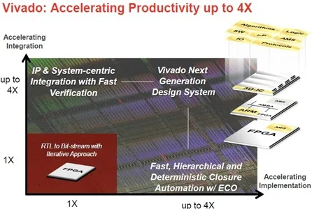
Xilinx Inc. has announced the Vivado Design Suite. It enables an IP and system centric next generation design environment. Especially meant for the next decade of ‘All-Programmable’ devices, it also accelerates the integration and implementation up to 4X. And, why now? That’s because the all-programmable devices enable programmable systems ‘integration.

Xilinx_VivadoThere are system integration bottlenecks, such as design and IP re-use, integrating algorithmic and RTL level IP, mixing DSP, embedded, connectivity and logic, and verification of blocks and “systems”.
There are implementation bottlenecks as well, such as hierarchical chip planning, multi-domain and multi-die physical optimization, predictable ‘design’ vs. ‘timing’ closure, and late ECOs and rippling effect of changes.
Vivado accelerates productivity up to 4X. The design suite elements include an integrated design environment, has a shared scalable data model, is scalable to 100 million gates, and debug and analysis. It shares design information between implementation steps that ensures fast convergence and timing closure. This enables highly efficient memory utilization. Also, it is scalable to future families, that are greater than 10 million logic cells (100 million gates) and enables cross-probing across the entire design.
Vivado also enables packaging designs into system-level IP for re-use. You can share IP within your team, project or company. Any 3rd party IP is delivered with a common look and feel. You can re-use IP at any point in the implementation process. The IP can be source, placed, or placed and routed.

Friday, 23 December 2011

Compiling Xilinx library for ModelSim simulator

It was all running cool with VHDL but when i tried to do post Place and Route simulation using SDF file of my design i stuck with following errors:

# ** Error: (vsim-SDF-3250) mips_struct.sdf(18): Failed to find INSTANCE '/top/dut/U1262'.
# ** Error: (vsim-SDF-3250) mips_struct.sdf(19): Failed to find INSTANCE '/top/dut/U1262'.
# ** Error: (vsim-SDF-3250) mips_struct.sdf(20): Failed to find INSTANCE '/top/dut/U1262'.
# ** Error: (vsim-SDF-3250) mips_struct.sdf(21): Failed to find INSTANCE '/top/dut/U1261'.
# ** Error: (vsim-SDF-3250) mips_struct.sdf(22): Failed to find INSTANCE '/top/dut/U1261'

googling a lot i found that i need to compile xilinx libraries and had to map it with ModelSim to get it worked. For this u need to write CompXlib in your TCL window of Xilinx.

CompXLib uses the ModelSim "vmap" command for library mapping. If the ModelSim environment variable is set, then the ".ini" file pointed to by the environment variable is modified. If the variable is not set, a local (in the directory in which CompXLib is run) "modelsim.ini" file contains the library mappings from the "vmap" command issued by CompXLib. If the "modelsim.ini" file is not writeable, the "vmap" command will make a local copy of the "modelsim.ini" file and write the library mappings to this file.

I used the “compxlib” command but still it was not working for me. When i checked my modelsim.ini file I found that the libraries was not mapped so i write below command in the modelsim.ini file and finally i find all compiled xilinx libraries in my library window of modelsim.

UNISIMS_VER = C:\Xilinx\10.1\ISE\verilog\mti_se\unisims_ver
UNIMACRO_VER = C:\Xilinx\10.1\ISE\verilog\mti_se\unimacro_ver
UNI9000_VER = C:\Xilinx\10.1\ISE\verilog\mti_se\uni9000_ver
SIMPRIMS_VER = C:\Xilinx\10.1\ISE\verilog\mti_se\simprims_ver
XILINXCORELIB_VER = C:\Xilinx\10.1\ISE\verilog\mti_se\XilinxCoreLib_ver
SECUREIP = C:\Xilinx\10.1\ISE\vhdl\mti_se\secureip
AIM_VER = C:\Xilinx\10.1\ISE\verilog\mti_se\abel_ver\aim_ver
CPLD_VER = C:\Xilinx\10.1\ISE\verilog\mti_se\cpld_ver
UNISIM = C:\Xilinx\10.1\ISE\vhdl\mti_se\unisim
UNIMACRO = C:\Xilinx\10.1\ISE\vhdl\mti_se\unimacro
SIMPRIM = C:\Xilinx\10.1\ISE\vhdl\mti_se\simprim
XILINXCORELIB = C:\Xilinx\10.1\ISE\vhdl\mti_se\XilinxCoreLib
AIM = C:\Xilinx\10.1\ISE\vhdl\mti_se\abel\aim
PLS = C:\Xilinx\10.1\ISE\vhdl\mti_se\abel\pls
CPLD = C:\Xilinx\10.1\ISE\vhdl\mti_se\cpld

** C:\Xilinx\10.1 is path in my system. Please check paths and make changes accordingly.

alternatively you can also use following commands

compxlib -s mti_se -arch virtex -lib unisim -lib simprim -lib xilinxcorelib -l vhdl -dir C:\Mentor\libraries\xilinx\10.1\ISE_Lib\ -log compxlib.log -w
compxlib -s mti_se -arch virtex2p -lib unisim -lib simprim -lib xilinxcorelib -l vhdl -dir C:\Mentor\libraries\xilinx\10.1\ISE_Lib\ -log compxlib.log -w
compxlib -s mti_se -arch virtex4 -lib unisim -lib simprim -lib xilinxcorelib -l vhdl -dir C:\Mentor\libraries\xilinx\10.1\ISE_Lib\ -log compxlib.log -w
compxlib -s mti_se -arch spartan3 -lib unisim -lib simprim -lib xilinxcorelib -l vhdl -dir C:\Mentor\libraries\xilinx\10.1\ISE_Lib\ -log compxlib.log -w
compxlib -s mti_se -arch virtex5 -lib unisim -lib simprim -lib xilinxcorelib -l vhdl -dir C:\Mentor\libraries\xilinx\10.1\ISE_Lib\ -log compxlib.log –w

**(C:\Mentor\libraries\xilinx\10.1\ISE_Lib\  is my path, you can use your own)

Saturday, 29 October 2011

Xilinx’s New Virtex-7 2000T FPGA with equivalent of 20 million ASIC gates

Xilinx has announced the first shipments of its Virtex-7 2000T Field Programmable Gate Array (FPGA). The Virtex-7 2000T is the world’s highest-capacity programmable logic device – it contains 6.8 billion transistors, providing customers access to 2 million logic cells. This is equivalent to 20 million ASIC gates, which makes these devices ideal for system integration, ASIC replacement, and ASIC prototyping and emulation.
This capacity is made possible by Xilinx’s Stacked Silicon Interconnect technology – also referred to as 2.5D ICs. The simplest packaging technology is to have a single die in the package. The next step up the “complexity ladder” is to have multiple die is the same package, but for all of these die to be attached directly to the package substrate. In this case, compared to the tracks on the die, the tracks on the package substrate are relatively large, slow, and driving signals onto them consumes a lot of power.
What Xilinx are doing is to go one more step up the technology ladder to use a special layer of silicon known as a "silicon interposer" combined with Through-Silicon Vias (TSVs). In this first incarnation of the technology, four FPGA die are attached to the silicon interposer, which – in addition to connecting the FPGAs to each other – provides connections to the package as illustrated below.

xilinx-bc-00

In the case of the Virtex-7 2000T, the FPGA die are implemented at the 28 nm technology node, while the passive silicon interposer is implemented at the 65 nm technology node. Implementing the large silicon interposer at this higher node reduces costs and increases yield without significantly degrading performance.
One way to think about this is that the silicon interposer essentially adds four additional tracking layers that can be used to connect the FPGAs to each other with more than 10,000 connections between each pair of adjacent die!
On top of this, Through-Silicon Vias (TSVs) are used to pass signals through the silicon interposer to C4 bumps on the bottom of the interposer. These bumps are then used to connect the interposer to the package substrate.

A view of Xilinx’s Virtex-7 2000T device showing the
packaging substrate (bottom), silicon interposer (middle),
and four FPGA die (top).

Compared with having to use standard I/O connections to integrate two FPGAs together on a circuit board, this stacked silicon interconnect technology is said to provide over 100X the die-to-die connectivity bandwidth-per-watt, at one-fifth the latency, without consuming any of the FPGAs' high-speed serial or parallel I/O resources.
Of particular interest to designers is the fact that, despite being composed of four die, the Virtex-7 2000T preserves the traditional FPGA use model in that users will program the device as one extremely large FPGA with the Xilinx tool flow and methodology.
Xilinx’s first application of 2.5D IC stacking gives customers twice the capacity of competing devices and leaps ahead of what Moore’s Law could otherwise offer in a monolithic 28-nanometer (nm) FPGA. Xilinx says that its customers can use Virtex-7 2000T FPGAs to replace large capacity ASICs to achieve overall comparable total costs in a third of the time, creating integrated systems that increase system bandwidth and reduce power by eliminating I/O interconnect, and accelerating the prototyping and emulation of advanced ASIC systems.

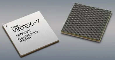
xilinx-bc-02A top and bottom view of Xilinx’s Virtex-7 2000T
device,
the world’s highest-capacity FPGA using
Stacked Silicon Interconnect technology.

“The Virtex-7 2000T FPGA marks a major milestone in Xilinx’s history of innovation and industry collaboration,” said Victor Peng, Xilinx Senior Vice President, Programmable Platforms Development. “Of significance to our customers is the fact that Stacked Silicon Interconnect technology offers capacities that otherwise wouldn’t be possible in an FPGA for at least another process generation. They can immediately add new functionality to existing designs while forgoing an ASIC, cost reduce a 3 or 5 FPGA solution into a single FPGA or move ahead with prototyping and building system emulators using our largest FPGAs at least a year earlier than typical for a new generation.”
Historically, the largest devices that make up an FPGA family are the last to be made available to customers.  This is a result of the time it takes a new semiconductor process to ramp up and support the yields per wafer that make the largest devices economically viable. Xilinx’s Stacked Silicon Interconnect technology overcomes the challenges of yielding defect-free, large monolithic die by building the world’s largest capacity programmable logic device from four separate FPGA die interconnected upon a passive silicon interposer.
“ARM is pleased to work with Xilinx in deploying the class-leading Virtex-7 2000T device into our validation infrastructure,” said John Goodenough, Vice President Design Technology and Automation, ARM. “The new device underpins a flexible, yet targeted, emulation architecture and delivers a significant capacity improvement, allowing us to more easily run complete system verification and validation for our next generation processors.”
The Virtex-7 2000T device also provides equipment manufacturers with an integration platform that will help them overcome the challenges of lowering power while increasing performance and capabilities. By eliminating the I/O interfaces between different ICs on a circuit board, a system’s overall power consumption can be reduced considerably.
Consider the following example provided by Xilinx that compares a single Virtex-7 2000T with four of the largest monolithic ICs as illustrated below:


xilinx-bc-00b

Actually, this is not really a fair comparison, because in terms of capacity the Virtex-7 2000T is equivalent to only around two of the largest monolithic ICs. But even comparing to two monolithic ICs results in a significant power advantage. (Having said this, I’d be interested to know just what was being exercised in this example – Logic? Memory? DSP slices? SERDES channels? – and at what frequency.)
Customers can also lower bill-of-material, test and development cycle costs when fewer IC devices are required on a circuit board. Because the die align side by side on a silicon interposer, this technology avoids the power and reliability issues that can result from stacking multiple dies on top of each other.  As was previously noted, the interposer includes over 10,000 high speed interconnects between each die enabling the high-performance integration required for a wide range of applications.
The Virtex-7 2000T FPGA gives customers the capacity, performance and power typically only found in large capacity ASICs, with the added benefits of re-programmability. In addition to having 1,954,560 logic cells, the Virtex-7 2000T device includes configurable logic blocks totaling 305,400 CLB slices and max distributed RAM of 21,550 Kbits. It has 2,160 DSP slices, 1,292 x 36Kb BRAMs (giving a total of 46,512 Kb of BRAM), 24 clock management tiles, four PCIe blocks and 36 GTX transceivers (each capable of 12.5 Gbits/second). It also has 24 I/O banks and a total of 1,200 user I/Os.
For the growing number of systems and markets where economics work against ASIC development, the Virtex-7 2000T FPGA offers a unique, scalable alternative to the risk of re-spins and more than $50 million in non-reoccurring engineering (NRE) costs of a 28nm custom-made IC.
All Xilinx 28nm devices – Artix-7, Kintex-7, Virtex-7 FPGAs, and the Zynq-7000 EPP – share a unified architecture that supports design and IP reuse within and across families. They are all built on TSMC’s 28nm HPL (low power with HKMG) process to deliver FPGAs that consume 50 percent less static power than competing devices. Because lower static power becomes increasingly important as device capacity goes up, 28nm HPL is a key factor behind the Virtex-7 2000T device’s lower power consumption compared to designs implemented in multiple FPGAs.

Xilinx Shatters Record with World's Highest Capacity FPGA: Virtex-7 2000T

The Virtex®-7 2000T FPGA is the first device to use 2.5-D IC stacked silicon interconnect technology to deliver "More than Moore" capacity: 2 million logic cells, 6.8 billion transistors - 2x the capacity of the largest competing device.

World’s Highest Capacity FPGA - Now Shipping

The Virtex®-7 2000T FPGA delivers greater than 2X the capacity and bandwidth offered by the largest monolithic devices while delivering the time-to-volume advantages of smaller die. Utilizing innovative 2.5D Stacked Silicon Interconnect (SSI) technology, the Virtex-7 2000T FPGA integrates 2 million logic cells, 6.8 billion transistors and 12.5Gb/s serial transceivers on a single device making it the world’s highest capacity FPGA offering unprecedented system integration in addition to ASIC prototyping and ASIC replacement capabilities.

Industry's Highest System Performance

Virtex-7 FPGAs are optimized for advanced systems requiring the highest performance and highest bandwidth connectivity. The Virtex-7 family is one of three product families built on a common 28nm architecture designed for maximum power efficiency and delivers 2X higher system performance at 50% lower power than previous generation FPGAs.

The Virtex-7 family consists of T, XT and HT devices to meet a wide array of market requirements:

Virtex-7 T devices deliver unprecedented levels of capacity and performance enabling ASIC prototyping, emulation and replacement

  • Up to 2M logic cells, 6.8 billion transistors and 12.5Gb/s serial transceivers on a single device
  • Enables non-linear integration to reduce board space, lower power and increase system performance
  • Delivers highest bandwidth, lowest latency by eliminating multiple chip bottlenecks
  • Enables rapid development and emulation of advance node ASICs

Virtex-7 XT devices offer the highest processing bandwidth with high performance transceivers, DSP and BRAM

  • Integrates up to 96 10G Base KR  backplane capable  serial transceivers
  • 5.3 TMACs of DSP 
  • 67 Mbits of internal memory
  • >1M logic cells

Virtex-7 HT devices with integrated 28Gbps serial transceivers offer an unprecedented 2.8Tb/s of serial bandwidth

  • Up to 16 x 28 Gb/s serial transceivers for ultra-high bandwidth applications
  • Optimized for next-generation 100G, nx100G and 400G line cards with CFP2 optical interfaces
  • Superior jitter performance to exceed CEI 28G specifications

EasyPath™-7 devices offer a conversion-free path to volume production.

Unified Architecture Enables Scalability and Increases Productivity

Fabricated on a high-performance, low-power (HPL) 28nm process, all 7 series FPGAs share a unified architecture. This innovation enables design migration across the Artix™-7, Kintex™-7, and Virtex-7 families. System manufacturers can easily scale successful designs to address adjacent markets requiring reduced cost and power or increased performance and capability. The adoption of AMBA 4, AXI4 specification as part of the interconnect strategy supporting Plug-and-Play FPGA design further improves productivity with IP reuse, portability, and predictability.

Virtex-7 FPGA Key Capabilities

Maximum Capability

Virtex-7 T Devices

Virtex-7 XT Devices

Virtex-7 HT Devices

Logic density (Logic Cells)

1,955K

1,139K

864K

Peak transceiver speed

12.5Gb/s
(GTX)

13.1Gb/s
(GTH)

28.05Gb/s
(GTZ)

Transceivers

36

96

88

Peak bi-directional serial bandwidth

0.900 Tb/s

2.515Tb/s

2.784Tb/s

DSP throughput (symmetric filter)

2,756 GMACS

5,314 GMACS

5,053 GMACS

Block RAM

46.5Mb

85.0Mb

64.4Mb

PCI Express® interface

Gen2x8

Gen3x8

Gen3x8

I/O pins

1,200

1,100

700

System Solutions Enabled by Virtex-7 FPGAs

Delivering the highest bandwidth with the lowest power, Virtex-7 FPGAs address the insatiable demand for networking infrastructure bandwidth. Delivering up to 2.8Tb/s serial bandwidth, these devices enable communications equipment manufacturers to increase network capacity with next-generation hardware that operates within existing power and cooling footprints.

See How Virtex-7 FPGAs Will Benefit Your Next Design

Application

Description

ASIC Prototyping

Build a highly integrated ASIC prototyping solution with the Virtex-7 2000T. With its high logic and processing capacity, mitigate development risks for large ASIC and ASSP designs.

2x100G OTU4 Transponder/Line Card

Build a 2x100G OTU4 Transponder/Line Card using the only 28nm FPGAs that enable designers to integrate two 100G interfaces into a single FPGA for reduced board space, power, and cost.

10GPON/10GEPON OLT Line Card

Meet aggressive 10G port count integration and cost targets for Passive Optical Network (PON) Optical Line Terminal (OLT) Line Cards that bring high-speed networking to the neighborhood/home.

100GE Line Card

Virtex-7 FPGAs offer the right mix of I/O, memory and logic to enable a single-FPGA implementation of new line cards that deliver increased bandwidth.

100G OTN Muxponder

Virtex-7 FPGA XT devices enable a flexible, single-FPGA, 100G OTN Multiplexing Transponder implementation.

300G Interlaken Bridge

Create a 300G Interlaken Bridge that enables infrastructure scaling with devices that deliver up to 1.9Tbps bandwidth for bridging between MAC-NPU, NPU-Switch, NPU-TCAM using the Interlaken industry standard.

400G Line Card

Be first to market with 400GE Line Cards by designing with the only FPGAs to support 400G serial interfaces with next-generation optics.

Portable RADAR Systems

Enable high performance RADAR systems through low power, multi-channel signal recovery and processing.

Terabit Switch Fabric

Virtex-7 FPGA XT device capabilities enable Terabit Switch Fabric to support proliferating 40G/100G ports in networking infrastructure.

Key Documents

Name

Modified

Size

7 Series FPGAs Overview

09/13/2011

563 KB

7 Series Product Brief


WP385 - Industry’s Highest Bandwidth FPGA Enables World’s First Single-FPGA Solution for 400G Communications Line Cards

11/22/2010

623 KB

WP312 - Xilinx Next Generation 28 nm FPGA Technology Overview

03/26/2011

614 KB

WP389 - Lowering Power at 28 nm with Xilinx 7 Series FPGAs

06/13/2011

1.13 MB

WP380 - Xilinx Stacked Silicon Interconnect Technology Delivers Breakthrough FPGA Capacity, Bandwidth, and Power Efficiency

10/21/2011

2.31 MB

WP373 - Xilinx Redefines Power, Performance, and Design Productivity with Three Innovative 28 nm FPGA Families: Virtex-7, Kintex-7, and Artix-7 Devices

10/11/2011

301 KB

Source : http://www.xilinx.com/