Featured post

Top 5 books to refer for a VHDL beginner

VHDL (VHSIC-HDL, Very High-Speed Integrated Circuit Hardware Description Language) is a hardware description language used in electronic des...

Thursday, 26 May 2011

NAND Gates


NAND gates have two bits of input and a single bit of output.
Since NAND is not associative, the definition is based on AND.

In particular

NANDk(x1, x2,...,xn) = NOT( ANDk(x1, x2,...,xn) )


Thus, NANDk is the negation of ANDk.

The truth table defines the behavior of this gate. It's the negation of AND.


The function implemented by NAND gates has interesting properties:

The function is symmetric. Thus, x NAND y == y NAND x. This can be verified by using truth tables.

The function is not associative. This can be verified by using truth tables.
Because of these properties, NANDk is defined from ANDk, and not built from NAND gates.

Wednesday, 25 May 2011

OR Gates


OR gates have two bits of input and a single bit of output.

The output of OR gate is logic '0' only if both inputs are logic '0'. Otherwise, the output is logic '1'.


The truth table defines the behavior of this gate.


The function implemented by OR gates has interesting properties:

The function is symmetric. Thus, x + y == y + x. This can be verified by using truth tables. We use "+" to represent OR.

The function is associative. Thus, (x + y) + z == x + (y + z). This can be verified by using truth tables.
Because of these properties, it's easy to define an n-input OR gate.

ORn(x1, x2,...,xn) = x1 + x2 + ... + xn
That is, an OR gate with n-inputs is the OR of all the bits. This is not ambiguous because the OR function is associative (all parenthesization of this expression are equivalent).

AND Gates


An AND gate have two bits of input and a single bit of output.
The output of AND gate is logic '1' only if both inputs are at logic '1'. Otherwise, the output is logic '0'.


The truth table defines the behavior of this gate.


The function implmented by AND2 gates has interesting properties:

The function is symmetric. Thus, x * y == y * x. This can be verified by using truth tables. We use * to represent AND.

The function is associative. Thus, (x * y) * z == x * (y * z). This can be verified by using truth tables.
Because of these properties, it's easy to define an n-input AND gate.

ANDn(x1, x2,...,xn) = x1 * x2 * ... * xn

That is, an AND gate with n-inputs is the AND of all the bits. This is not ambiguous because the AND function is associative (all parenthesization of this expression are equivalent).

VHDL code for AND gate

Logic NOT Gate


Logic Gates

The Logic “NOT” Gate

Logic NOT Gate Definition

The digital Logic NOT Gate is the most basic of all the logical gates and is sometimes referred to as an Inverting Buffer or simply a Digital Inverter. It is a single input device which has an output level that is normally at logic level “1” and goes “LOW” to a logic level “0” when its single input is at logic level “1”, in other words it “inverts” (complements) its input signal. The output from a NOT gate only returns “HIGH” again when its input is at logic level “0” giving us the Boolean expression of:  A = Q.
Then we can define the operation of a single input Digital Logic NOT Gate as being:

“If A is NOT true, then Q is true”

Transistor NOT Gate


A simple 2-input logic NOT gate can be constructed using a RTL Resistor-transistor switches as shown below with the input connected directly to the transistor base. The transistor must be saturated “ON” for an inverted output “OFF” at Q.

The Logic NOT Gate Truth Table

Symbol
Truth Table
Inverter or NOT Gate
A
Q
0
1
1
0
Boolean Expression Q = not A or A
Read as inverse of A gives Q

Logic NOT gates provide the complement of their input signal and are so called because when their input signal is “HIGH” their output state will NOT be “HIGH”. Likewise, when their input signal is “LOW” their output state will NOT be “LOW”. As they are single input devices, logic NOT gates are not normally classed as “decision” making devices or even as a gate, such as the AND or OR gates which have two or more logic inputs. Commercial available NOT gates IC’s are available in either 4 or 6 individual gates within a single IC package.
The “bubble” (o) present at the end of the NOT gate symbol above denotes a signal inversion (complementation) of the output signal. But this bubble can also be present at the gates input to indicate an active-LOW input. This inversion of the input signal is not restricted to the NOT gate only but can be used on any digital circuit or gate as shown with the operation of inversion being exactly the same whether on the input or output terminal. The easiest way is to think of the bubble as simply an inverter.

Signal Inversion using Active-low input Bubble


Bubble Notation for Input Inversion

NAND and NOR Gate Equivalents

An Inverter or logic NOT gate can also be made using standard NAND and NOR gates by connecting together ALL their inputs to a common input signal for example.


A very simple inverter can also be made using just a single stage transistor switching circuit as shown. When the transistors base input at “A” is high, the transistor conducts and collector current flows producing a voltage drop across the resistor R thereby connecting the output point at “Q” to ground thus resulting in a zero voltage output at “Q”.

Likewise, when the transistors base input at “A” is low (0v), the transistor now switches “OFF” and no collector current flows through the resistor resulting in an output voltage at “Q” high at a value near to +Vcc.

Then, with an input voltage at “A” HIGH, the output at “Q” will be LOW and an input voltage at “A” LOW the resulting output voltage at “Q” is HIGH producing the complement or inversion of the input signal.


Hex Schmitt Inverters


A standard Inverter or Logic NOT Gate, is usually made up from transistor switching circuits that do not switch from one state to the next instantly, there will always be some delay in the switching action.
Also as a transistor is a basic current amplifier, it can also operate in a linear mode and any small variation to its input level will cause a variation to its output level or may even switch “ON” and “OFF” several times if there is any noise present in the circuit. One way to overcome these problems is to use a Schmitt Inverter or Hex Inverter.
We know from the previous pages that all digital gates use only two logic voltage states and that these are generally referred to as Logic “1” and Logic “0” any TTL voltage input between 2.0v and 5v is recognised as a logic “1” and any voltage input below 0.8v is recognised as a logic “0” respectively.
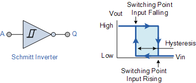
A Schmitt Inverter is designed to operate or switch state when its input signal goes above an “Upper Threshold Voltage” or UTV limit in which case the output changes and goes “LOW”, and will remain in that state until the input signal falls below the “Lower Threshold Voltage” or LTV level in which case the output signal goes “HIGH”. In other words a Schmitt Inverter has some form of Hysteresis built into its switching circuit.
This switching action between an upper and lower threshold limit provides a much cleaner and faster “ON/OFF” switching output signal and makes the Schmitt inverter ideal for switching any slow-rising or slow-falling input signal and as such we can use a Schmitt trigger to convert these analogue signals into digital signals as shown.

Schmitt Inverter


A very useful application of Schmitt inverters is when they are used as oscillators or sine-to-square wave converters for use as square wave clock signals.

Schmitt NOT Gate Inverter Oscillator


The first circuit shows a very simple low power RC type oscillator using a Schmitt inverter to generate a square wave output waveform. Initially the capacitor C is fully discharged so the input to the inverter is “LOW” resulting in an inverted output which is “HIGH”. As the output from the inverter is fed back to its input and the capacitor via the resistor R the capacitor begins to charge up.
When the capacitors charging voltage reaches the upper threshold limit of the inverter, the inverter changes state, the output becomes “LOW” and the capacitor begins to discharge through the resistor until it reaches the lower threshold level were the inverter changes state again. This switching back and forth by the inverter produces a square wave output signal with a 33% duty cycle and whose frequency is given as: ƒ = 680/RC.
The second circuit converts a sine wave input (or any oscillating input for that matter) into a square wave output. The input to the inverter is connected to the junction of the potential divider network which is used to set the quiescent point of the circuit. The input capacitor blocks any DC component present in the input signal only allowing the sine wave signal to pass.
As this signal passes the upper and lower threshold points of the inverter the output also changes from “HIGH” to “LOW” and so on producing a square wave output waveform. This circuit produces an output pulse on the positive rising edge of the input waveform, but by connecting a second Schmitt inverter to the output of the first, the basic circuit can be modified to produce an output pulse on the negative falling edge of the input signal.
Commonly available logic NOT gate and Inverter IC’s include:
TTL Logic NOT Gates
  • 74LS04 Hex Inverting NOT Gate
  • 74LS14 Hex Schmitt Inverting NOT Gate
  • 74LS1004 Hex Inverting Drivers

CMOS Logic NOT Gates
  • CD4009 Hex Inverting NOT Gate
  • CD4069 Hex Inverting NOT Gate

7404 NOT Gate or Inverter


Saturday, 14 May 2011

Toward faster transistors

MIT physicists discover a new physical phenomenon that could eventually lead to the first increases in computers’ clock speed since 2002.


In the 1980s and ’90s, competition in the computer industry was all about “clock speed” — how many megahertz, and ultimately gigahertz, a chip could boast. But clock speeds stalled out almost 10 years ago: Chips that run faster also run hotter, and with existing technology, there seems to be no way to increase clock speed without causing chips to overheat.

In this week’s issue of the journal Science, MIT researchers and their colleagues at the University of Augsburg in Germany report the discovery of a new physical phenomenon that could yield transistors with greatly enhanced capacitance — a measure of the voltage required to move a charge. And that, in turn, could lead to the revival of clock speed as the measure of a computer’s power.

In today’s computer chips, transistors are made from semiconductors, such as silicon. Each transistor includes an electrode called the gate; applying a voltage to the gate causes electrons to accumulate underneath it. The electrons constitute a channel through which an electrical current can pass, turning the semiconductor into a conductor.

Capacitance measures how much charge accumulates below the gate for a given voltage. The power that a chip consumes, and the heat it gives off, are roughly proportional to the square of the gate’s operating voltage. So lowering the voltage could drastically reduce the heat, creating new room to crank up the clock.

Shoomp!

MIT Professor of Physics Raymond Ashoori and Lu Li, a postdoc and Pappalardo Fellow in his lab — together with Christoph Richter, Stefan Paetel, Thilo Kopp and Jochen Mannhart of the University of Augsburg — investigated the unusual physical system that results when lanthanum aluminate is grown on top of strontium titanate. Lanthanum aluminate consists of alternating layers of lanthanum oxide and aluminum oxide. The lanthanum-based layers have a slight positive charge; the aluminum-based layers, a slight negative charge. The result is a series of electric fields that all add up in the same direction, creating an electric potential between the top and bottom of the material.

Ordinarily, both lanthanum aluminate and strontium titanate are excellent insulators, meaning that they don’t conduct electrical current. But physicists had speculated that if the lanthanum aluminate gets thick enough, its electrical potential would increase to the point that some electrons would have to move from the top of the material to the bottom, to prevent what’s called a “polarization catastrophe.” The result is a conductive channel at the juncture with the strontium titanate — much like the one that forms when a transistor is switched on. So Ashoori and his collaborators decided to measure the capacitance between that channel and a gate electrode on top of the lanthanum aluminate.

They were amazed by what they found: Although their results were somewhat limited by their experimental apparatus, it may be that an infinitesimal change in voltage will cause a large amount of charge to enter the channel between the two materials. “The channel may suck in charge — shoomp! Like a vacuum,” Ashoori says. “And it operates at room temperature, which is the thing that really stunned us.”

Indeed, the material’s capacitance is so high that the researchers don’t believe it can be explained by existing physics. “We’ve seen the same kind of thing in semiconductors,” Ashoori says, “but that was a very pure sample, and the effect was very small. This is a super-dirty sample and a super-big effect.” It’s still not clear, Ashoori says, just why the effect is so big: “It could be a new quantum-mechanical effect or some unknown physics of the material.”

“For capacitance, there is a formula that was assumed to be correct and was used in the computer industry and is in all the textbooks,” says Jean-Marc Triscone, a professor of physics at the University of Geneva whose group has published several papers on the juncture between lanthanum aluminate and strontium titanate. “What the MIT team and Mannhart showed is that to describe their system, this formula has to be modified.”

There is one drawback to the system that the researchers investigated: While a lot of charge will move into the channel between materials with a slight change in voltage, it moves slowly — much too slowly for the type of high-frequency switching that takes place in computer chips. That could be because the samples of the material are, as Ashoori says, “super dirty”; purer samples might exhibit less electrical resistance. But it’s also possible that, if researchers can understand the physical phenomena underlying the material’s remarkable capacitance, they may be able to reproduce them in more practical materials.

Triscone cautions that wholesale changes to the way computer chips are manufactured will inevitably face resistance. “So much money has been injected into the semiconductor industry for decades that to do something new, you need a really disruptive technology,” he says.

“It’s not going to revolutionize electronics tomorrow,” Ashoori agrees. “But this mechanism exists, and once we know it exists, if we can understand what it is, we can try to engineer it.”


Source : http://web.mit.edu

Sunday, 8 May 2011

VLSI Interview Questions-1


1.What is the difference between mealy and moore state-machines.
2.How to solve setup and hold violations in the design.
3.What is antenna violation & ways to prevent it.
4.We have multiple instances in RTL(Register Transfer Language), do you do anything special during synthesis stage.
5.What is tie-high and tie-low cells and where it is used.
6.What is the difference between latches and flip-flops based designs.
7.What is High-Vt and Low Vt cells.
8.What is LEF mean?
9.What is DEF mean?
10.Steps involved in designing an optimal padring.
11.What is metastability and steps to prevent it.
12.What is local-skew, global skew and useful skew.
13.What are the various timing-paths which i should take care in my STA runs?
14.What are the various components of leakage-power.
15.What are the various yield losses in the design.
16.What is meant by virtual clock definition and why do i need it.
17.What are the various variations which impacts timing of the design.
18.What are the various Design constraints used, while performing synthesis for a design.
19.Specify few verilog constructs which are not supported by the synthesis tool.
20.What are the various capacitances with an MOSFET?
21.Vds-Ids curve for an MOSFET, with increasing Vgs.
22.Explain basic operation of an MOSFET.
23.what is channel length modulation.
24.what is body effect.
25.what is latchup in CMOS design and ways to prevent it?
26.what are the various design changes you do to meet design power targets.
27.what is meant by library characterization.
28.what is meant by wireload model.
29.what are the measures to be taken to design for optimized area.
30.what all will you be thinking while performing floorplan.
31.what are the measures in the design taken for meeting signal integrity targets.
32.what are the measures taken in the Design achieving better yield.
33.what are the measures or precautions to be taken in the design when the chip has both analog and digital portions..
34.what are the steps incorporated for Engineering Change order[ECO].
35.what are the steps performed to achieve Lithography friendly Design.
36.what does synthesis mean?
37.what are the pre-requistes to perform synthesis.
38.Can you explain the synthesis flow.
39.what are the various ways to reduce clock insertion delay in the design.
40.what are the various functional verification methodologies.
41.what does formal verification mean.
42.How will you time the output path in STA.
43.How will you time the input path in STA.
44.What is false path mean in STA and in what scenarios falsepath can come.
45.What does multicycle path mean in STA and in what scenarios MCP can come.
46.What are source synchronous paths in STA.
47.Assume there is a specific requirement to preserve the logic during synthesis , how will you achieve it..
48.we have multiple instances in RTL, do you do anything special during synthesis stage.
49.What do you call an event and when do you call an assertion.

Thursday, 5 May 2011

ISRO Builds India's Fastest Supercomputer

Indian Space Research Organisation has built a supercomputer, which is to be India's fastest supercomputer in terms of theoretical peak performance of 220 TeraFLOPS (220 Trillion Floating Point Operations per second). The supercomputing facility named as Satish Dhawan Supercomputing Facility is located at Vikram Sarabhai Space Centre (VSSC), Thiruvananthapuram. The new Graphic Processing Unit (GPU) based supercomputer named "SAGA-220" (Supercomputer for Aerospace with GPU Architecture-220 TeraFLOPS) is being used by space scientists for solving complex aerospace problems. The supercomputer SAGA-220 was inaugurated by Dr K Radhakrishnan, Chairman, ISRO today at VSSC.

"SAGA-220" Supercomputer is fully designed and built by Vikram Sarabhai Space Centre using commercially available hardware, open source software components and in house developments. The system uses 400 NVIDIA Tesla 2070 GPUs and 400 Intel Quad Core Xeon CPUs supplied by WIPRO with a high speed interconnect. With each GPU and CPU providing a performance of 500 GigaFLOPS and 50 GigaFLOPS respectively, the theoretical peak performance of the system amounts to 220 TeraFLOPS. The present GPU system offers significant advantage over the conventional CPU based system in terms of cost, power and space requirements. The total cost of this Supercomputer is about Rs. 14 crores. The system is environmentally green and consumes a power of only 150 kW. This system can also be easily scaled to many PetaFLOPS (1000 TeraFLOPS).