Featured post

Top 5 books to refer for a VHDL beginner

VHDL (VHSIC-HDL, Very High-Speed Integrated Circuit Hardware Description Language) is a hardware description language used in electronic des...

Tuesday, 13 May 2014

Motorola Moto E: Price, specifications, features and comparison


After leaving the Indian market in 2011, Motorola made a comeback last year with the Moto G, and how. Its first Smartphone post the comeback shook the Rs 10,000-Rs 15,000 segment in the country. Motorola’s retail model, where it only sells phone via Flipkart, may seem restricting to many, but that didn’t stop the Moto G to become the best selling Smartphone in the company’s history. The Moto G was followed by the flagship Moto X, which was in fact launched much before in August last year. The device priced in the Rs 20,000-Rs 25,000 range took a different path to its competitors — putting user experience ahead of the specification race. While its success may not have touched the dizzying heights of the Moto G, it nonetheless managed to impress many. Now, Motorola is back with another device, which too seems like a contender to shakeup the entry-level segment. Let’s have a detailed look at the Motorola Moto E.

MOTOROLA MOTO E PRICE IN INDIA
The Moto E is priced at Rs 6,999, which is quite aggressive. Motorola is focusing on changing the perception of entry-level devices and wants to offer first time Smartphone users a premium and well built device.

MOTOROLA MOTO E DESIGN
At first glance the Moto E looks quite similar to the Moto G, but look closer and you will see that the back panels have a different pattern, and there is no front-facing camera. In terms of dimensions, the Moto E (64.8×124.8×12.3mm) is shorter, less wide and slimmer than the Moto G (65.9×129.9×11.6mm)
The customization options include removable back panels, with up to nine different colored panels to choose from.

MOTOROLA MOTO E HARDWARE
DISPLAY – A 4.3-inch qHD display may not sound much, but you have to remember that no other tier-one company offers this kind of resolution in this price segment. The display is quite sharp and does a decent job in reproducing colors. Motorola has also added Corning Gorilla Glass 3 protection, which means the display won’t be easily scratched.

PROCESSOR – The device is powered by a Snapdragon 200 dual-core processor clocked at 1.2GHz and paired with Adreno 302 GPU. Motorola again gets one over its competitors by including a 1GB of RAM, where other companies only provide 512MB of RAM.

STORAGE – You get 4GB of internal storage of which only about 2.22GB is available for users. But on the plus side, there is a microSD card slot to expand the memory up to 32GB.

CAMERAS – There is a 5-megapixel rear camera, which is the same as the Moto G, but unfortunately it isn’t accompanied by a flash. The camera does an okay job at capturing images, but more often than now you would wish you had a flash. Selfie lovers won’t be happy to hear that there is no front camera.

BATTERY – There is a 1,980mAh battery, which the company claims is good enough to last for a day.

EXTRAS – Like the Moto G and the Moto X, the Moto E has a nano coating on the inside as well as the outside. The coating will ensure your device is protected from an occasional splash of water. The coating also ensures there aren’t any ugly flaps covering the ports.

CONNECTIVITY OPTIONS – Besides the usual connectivity options like 3G, Wi-Fi and Bluetooth, the Moto E also has dual-SIM card slots. The dual-SIM functionality is quite smart in the sense that it keeps monitoring your usage and then automatically selects the SIM based on the contact you are calling.

MOTOROLA MOTO E SOFTWARE
The Motorola Moto E runs on the latest Android 4.4.2 KitKat and Motorola has also promised that the device will get at least one more OS update. Additionally, Motorola has also introduced a host of new features like Moto Alert, Instant SMS and Emergency Mode. Moto Alert will automatically alert preset contacts when you leave a particular location, Instant SMS will send a text with your location to preset contacts in emergency situations, and in Emergency mode, the device will call a preset contact or sound an alarm.

MOTOROLA MOTO E FIRST IMPRESSIONS
We got to spend some time with the device and you can read our first impressions of the device here.

MOTOROLA MOTO E COMPARISONS
At the price point, the Moto E will be up against the likes of the Sony Xperia E1 Dual, Nokia X and the Samsung Galaxy S Duos 2 among others. All the devices feature dual-core processors, 4GB expandable memory and are priced under Rs 9,000. The Moto E has the best display in terms of resolution, most RAM (1GB) and the biggest battery. It also runs on the latest Android KitKat and will get a guaranteed update. In the photography department, only Samsung offers a VGA front facing camera, while the rest don’t have one.

FEATURES
MOTOROLA MOTO E
SONY XPERIA E1 DUAL
NOKIA X
SAMSUNG GALAXY S DUOS 2
DISPLAY
4.3-inch qHD 4-inch WVGA 4-inch WVGA 4-inch WVGA
PROCESSOR
1.2GHz Snapdragon 200 dual-core 1.2GHz Snapdragon 200 dual-core 1.2GHz Snapdragon S4 dual-core 1.2GHz dual-core
RAM
1GB 512MB 512MB 768MB
STORAGE
4GB expandable 4GB expandable 4GB expandable 4GB expandable
CAMERAS (REAR/FRONT)
5-megapixel/ - 3-megapixel/ - 3-megapixel/ - 5-megapixel/VGA
BATTERY
1,980mAh 1,700mAh 1,500mAh 1,500mAh
Operating System
Android 4.4.2 KitKat Android 4.3 Jelly Bean Nokia Software Platform Android 4.2 Jelly Bean
PRICE
Rs 6,999 Rs 8,363 Rs 6,955 Rs 8,305


Wednesday, 16 April 2014

Intel’s e-DRAM

When Intel launched their Haswell series chips last June, they stated that the high-end systems would have embedded DRAM, as a separate chip in the package; and they gave a paper at the VLSI Technology Symposium that month, and another at IEDM.
It took us a while to track down a couple of laptops with the requisite Haswell version, but we did and now we have a few images that show it’s a very different structure from the other e-DRAMs that we’ve seen.
IBM has been using e-DRAM for years, and in all of their products since the 45-nm node. They have progressed their trench DRAM technology to the 22-nm node [3], though we have yet to see that in production.Embedded DRAM in IBM Power 7+ (32-nm)
TSMC and Renesas have also used e-DRAM in the chips they make for the gaming systems, the Microsoft Xbox and the Nintendo Wii. They use a more conventional form of memory stack with polysilicon wine-glass-shaped capacitors. TSMC uses a cell-under-bit stack where the bitline is above the capacitors, and Renesas a cell-over-bit (COB) structure with the bitline below.
Embedded DRAM in Microsoft Xbox GPU fabbed by TSMC (65-mm)
Embedded DRAM in Nintendo Wii U GPU fabbed by Renesas (45-mm)
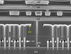
Intel also uses a COB stack, but they build a MIM capacitor in the metal-dielectric stack using a cavity formed in the lower metal level dielectrics. The part is fabbed in Intel’s 9-metal, 22-nm process:
General structure of Intel’s 22-nm embedded DRAM part from Haswell package
When we zoom in and look at the edge of the capacitor array, we can see that the M2 – M4 stack has been used to form the mould for the capacitors.Intel’s-22-nm-embedded-DRAM-stack
Looking a little closer, we can see the wordline transistors on the tri-gate fin, with passing wordlines at the end of each fin. Two capacitors contact each fin, and the bitline contact is in the centre of the fin.A closer look at the Intel 22-nm embedded DRAM stack
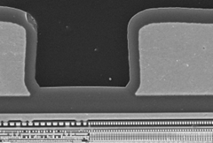
We can see some structure in the capacitors, but at the moment we have not done any materials analysis.  A beveled sample lets us view the plan-view:
Plan-view image of the Intel 22-nm embedded DRAM capacitors
The capacitors are clearly rectangular, but again in the SEM we cannot see any detailed structure. We’ll have to wait for further analysis with the TEM for that!
Intel claims a cell capacitance of more than 13 fF and a cell size of 0.029 sq. microns, so about a third of their 22-nm SRAM cell area of ~0.09 sq. microns, and a little larger than the IBM equivalent of 0.026 sq. microns. The wordline transistors are low-leakage trigate transistors with an enlarged contacted gate pitch of 108 nm (the minimum CGP is 90 nm). In the Haswell usage the die is used as a 128 MB L4 cache, with a die size of ~79 sq. mm, co-packaged with the CPU.
Intel got out of the commodity DRAM business almost thirty years ago; it will be interesting to see where they take their new entry, though not likely into competition with the big three suppliers. Their “Knights Landing” high-performance computing (HPC) platform is reported to use 16 GB of eDRAM, which will take the equivalent of 128 of these chips, so perhaps the future is in HPC and gaming systems such as the one we bought to get the part.


Saturday, 5 April 2014

Latch Up In CMOS

What is latch up in CMOS design and ways to prevent it?

A Problem which is inherent in the p-well and n-well processes is due to relatively large number of junctions which are formed in these structures, the consequent presence of parasitic diodes and transistors.

Latch-up is a condition in which the parasitic components give rise to the Establishment of low resistance conducting path between VDD and VSS with Disastrous results

Latch-up may be induced by glitches on the supply rails or by incident radiation.

Latch-up pertains to a failure mechanism wherein a parasitic thyristor (such as a parasitic silicon controlled rectifier, or SCR) is inadvertently created within a circuit, causing a high amount of current to continuously flow through it once it is accidentally triggered or turned on. Depending on the circuits involved, the amount of current flow produced by this mechanism can be large enough to result in permanent destruction of the device due to electrical overstress (EOS).

Preventions for Latch-Up

  • by adding tap wells, for example in an Inverter for NMOS add N+ tap in n-well and connect it to Vdd, and for PMOS add P+ tap in p-substrate and connect it to Vss.
  • an increase in substrate doping levels with a consequent drop in the value of  Rs.
  • reducing Rp by control of fabrication parameters and by ensuring a low contact resistance to Vss.
  • and the other is by introducing of guard rings.....

Latchup in Bulk CMOS

A byproduct of the Bulk CMOS structure is a pair of parasitic bipolar transistors. The collector of each BJT is connected to the base of the other transistor in a positive feedback structure. A phenomenon called latchup can occur when (1) both BJT's conduct, creating a low resistance path between Vdd and GND and (2) the product of the gains of the two transistors in the feedback loop, b1 x b2, is greater than one. The result of latchup is at the minimum a circuit malfunction, and in the worst case, the destruction of the device.

parasitic_transitor_in_bulk_cmos  Cross section of parasitic transistors in Bulk CMOS

parasitic_transitor_in_bulk_cmos_equivalent_circuit Equivalent Circuit

Latchup may begin when Vout drops below GND due to a noise spike or an improper circuit hookup (Vout is the base of the lateral NPN Q2). If sufficient current flows through Rsub to turn on Q2 (I Rsub > 0.7 V ), this will draw current through Rwell. If the voltage drop across Rwell is high enough, Q1 will also turn on, and a self-sustaining low resistance path between the power rails is formed. If the gains are such that b1 x b2 > 1, latchup may occur. Once latchup has begun, the only way to stop it is to reduce the current below a critical level, usually by removing power from the circuit.

The most likely place for latchup to occur is in pad drivers, where large voltage transients and large currents are present.

Preventing latchup

Fab/Design Approaches:

  1. Reduce the gain product b1 x b1
  • move n-well and n+ source/drain farther apart increases width of the base of Q2 and reduces gain beta2 ­> also reduces circuit density
  • buried n+ layer in well reduces gain of Q1

    2. Reduce the well and substrate resistances, producing lower voltage drops

· higher substrate doping level reduces Rsub

· reduce Rwell by making low resistance contact to GND

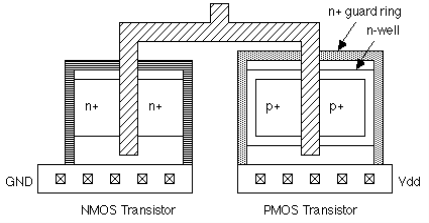
· guard rings around p- and/or n-well, with frequent contacts to the rings, reduces the parasitic resistances.

cmos_transitor_with_guard_rings CMOS transistors with guard rings

Systems Approaches:

  1. Make sure power supplies are off before plugging a board. A "hot plug in" of an unpowered circuit board or module may cause signal pins to see surge voltages greater than 0.7 V higher than Vdd, which rises more slowly to is peak value. When the chip comes up to full power, sections of it could be latched.
  2. Carefully protect electrostatic protection devices associated with I/O pads with guard rings. Electrostatic discharge can trigger latchup. ESD enters the circuit through an I/O pad, where it is clamped to one of the rails by the ESD protection circuit. Devices in the protection circuit can inject minority carriers in the substrate or well, potentially triggering latchup.
  3. Radiation, including x-rays, cosmic, or alpha rays, can generate electron-hole pairs as they penetrate the chip. These carriers can contribute to well or substrate currents.
  4. Sudden transients on the power or ground bus, which may occur if large numbers of transistors switch simultaneously, can drive the circuit into latchup. Whether this is possible should be checked through simulation.

Get free daily email updates!

Follow us!

Monday, 3 March 2014

Do U Know? Mobile devices said to consume more energy on storage tasks

28058-clipart-illustration-of-a-battery-mascot-cartoon-character-flexing-his-arm-musclesDo u know that “Flash storage takes power to write - a 20 volt jolt to each cell - but needs almost none to maintain. The real power hog is the inefficient storage software stack that eats 200 times the power required for the hardware.”

Given the always-on mobile infrastructure - background updates, instant messages, email, updates, file sync, logging and more - lots of background storage I/O is happening all the time. And it's eating your device's power budget.

Researchers from Microsoft and the University of California at San Diego benchmarked how Android and Windows RT mobile devices used energy for storing data. They focused on activities that occur with the screen off, since displays are a major power consumer when lit. "Measurements across a set of storage-intensive micro benchmarks show that storage software may consume as much as 200x more energy than storage hardware on an Android phone and a Windows RT tablet," the research team wrote in a paper. "The two biggest energy consumers are encryption and managed language environments."

Results
On Windows RT they found that the OS/CPU/DRAM overhead was between 5 and 200 times the power used by the flash storage itself, depending on how DRAM power use was allocated. File system APIs, the language environment and encryption drove the CPU power consumption during I/O. Full disk encryption - protecting user data - incurred 42 percent of CPU utilization.

On an Android phone, the encryption penalty is even worse: 2.6–5.9x more energy per KB over non-encrypted I/O.

For applications, the team found that on Windows RT, the energy overhead in a managed environment is 12.6–18.3 percent while overhead on Android is between 24.3–102.1 percent. It appears that Android's algorithms are not optimized for application I/O power efficiency.

Thursday, 27 February 2014

Assertion Debugging in Questa – few tips

Playing around debugging some complex assertions in Qeusta? Here are some tips:

1. Use vsim –assertdebug

2. Add –novopt for trivial code containing assertions + stim alone as otherwise many signals get optimized away. On real designs, perhaps you are better off with +acc* (Read doc for more)

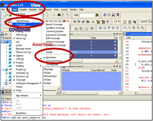
3. Once the GUI comes up, the assertions are not listed in its own browser – ideally I would have liked to see a menu item under “Tools” menu. But it is hidden under “View –> Coverage –> Assertions” – GOK why! (GOK – God Only Knows)  :)

4. Before starting simulation, enable ATV

5. After sim one can do “view ATV” for advanced debug!

Questa_dbg


Get free daily email updates!

Follow us!

Wednesday, 5 February 2014

Motorola Moto G Now In India


Motorola's much awaited Android smartphone Moto G has been launched in India at a price point of Rs 12,499 for the 8GB variant and Rs 13,999 for the 16GB storage variant.
The company took to twitter to confirm the news. "Moto G is now available in India, exclusively on Flipkart. Order it today to take advantage of launch offers," it said
Available exclusively on Flipkart initially, As a promotional gesture, the online retailer is offering Rs.500 discounts on e-Books, Rs.1000-off on the clothing, flat 70-percent off on cover-cases and some lucky  consumers will also stand a chance to win 100-percent cash back (in terms of store credit) with the purchase of Moto G. [offer is for limited period only]

At the moment the 16GB model has been listed on Flipkart ( with 1 year manufacturer warranty for Phone and 6 months warranty for in the box accessories Motorola India Warranty and Free Transit Insurance.)

Apart from Flipkart, Snapdeal is also retailing Moto G. As of now, the pre-order booking has been closed due non-availability of stocks. It recorded 1000 orders within 2 hours of listing the Moto G on 4 February, reported BGR.
Feature-rich Moto G flaunts a 4.5-inch HD (1270x720p) LCD screen protected by Corning Gorilla Glass 3 shield and houses dual-SIM slots. It run on the Android v4.3 Jelly Bean (guaranteed to get KitKat update) powered by a Qualcomm Snapdragon 400 series quad-core processor backed by 1GB RAM and comes in 8GG and 16GB variants.
With the launch, Motorola Moto G is expected to give a stiff challenge to low-cost Indian smartphones like Micromax Canvas Turbo Mini A200, Lava Iris Pro 30, Karbonn Titanium S5 plus and others.

Motorola G Specifications:

Model Motorola Moto G (Dual-SIM model confirmed for India)
Display 4.5-inch HD (1270x720p) LCD screen with 329 ppi (pixels per inch), comes protected with Corning Gorilla Glass 3 shield.
OS  Android v4.3, Guaranteed update of Android v4.4 KitKat
Processor Qualcomm Snapdragon 400 series quad-core processor with 1.2GHz CPU speed
RAM 1GB
Storage capacity 8GB/16 GB variants ( no microSD card slot)
Camera Main: 5.0-megapixel camera with LED flash
Front: 1.3-megapixel camera
Network 3G
Battery 2,070 mAh
Add-ons Wi-Fi (802.11 b/g/n),Bluetooth v4.0, USB, NFC, GPS
Dimensions 129.9 x 65.9 x 11.6 mm
Weight 143 g
Price 8GB: Rs.12,999 & 16GB: Rs.14,499

Saturday, 1 February 2014

ModelSim VS QuestaSim

We as an ASIC Engineer are frequently using different simulators for our simulation activity. At present time we are frequently using modelsim/Questa and vcs. These are the industry popular and well proven simulators.
We have seen people who are using modelsim / Questa simulator from Mentors but dont really know the exact difference between them.
We have captured some difference between Questa and Modelsim. Though both are simulators from the Mentor Graphics there are some differences between them. Below are the differences We captured :

ModelSim is Mentor Graphics HDL simulator. Questa is Mentor Graphics advanced verification platform that uses ModelSim as its core simulation engine.

Features of the two tools can be grouped into five categories and compared as follows:

1. Language Support
- ModelSim supports SystemVerilog IEEE 1800 for Design only, as well as VHDL (1987, 1993, 2002), Verilog (1995, 2001, 2005), as well as options for mixed language and language neutral licensing and support for SystemC 2.2 IEEE 1666/OSCI 2.2.
- Questa supports all of this as well as SystemVerilog IEEE 1800 for Verification, mixed language licensing (Questa is by default language neutral), PSL IEEE 1850, and SystemC 2.2 IEEE 1666/OSCI 2.2 as standard features.

2. Simulation
- ModelSim supports a single-kernel simulation engine, Verilog RTL & gate level performance optimizations, VHDL RTL & VITAL performance optimizations, performance and memory profiler, separate elaboration, waveform management tool set, VCD and extended VCD support, VCD re-simulation, batch mode simulation, integrated simulation, checkpoint & restore,
- Questa’s simulation support is identical to ModelSim’s

3. Design Entry, Debug, and Analysis
- ModelSim supports an HDL editor, integrated project manager, source code templates and wizards, interactive and post-simulation debug, dataflow graphical and textual causality traceback, source annotation, memory window, extra standalone viewer, multiple waveform windows, waveform compare, C Debugger and transaction viewing for SystemC.
- Questa supports all of this and the C debugger and transaction viewing for SystemC and SystemVerilog are standard parts of the product.

4. Advanced Verification Methods
- ModelSim does not support any advanced verification features.
- Questa supports assertion-based verification (including a library of pre-written assertions called Questa Verification Library or QVL, and an assertion thread debugger), automated test stimulus generation via a constraint solver engine, and PowerAware RTL verification supporting both CPF and UPF formats.

5 Verification Management and Coverage
- ModelSim supports Code Coverage (it is included in ModelSim SE, and an option to other versions of ModelSim).
-Questa supports code coverage along with functional coverage, a unified coverage database (UCDB), coverage viewing, test ranking, and test plan tracking

Hope you find this information useful.

Get free daily email updates!

Follow us!