Featured post
Top 5 books to refer for a VHDL beginner
VHDL (VHSIC-HDL, Very High-Speed Integrated Circuit Hardware Description Language) is a hardware description language used in electronic des...
Sunday, 11 September 2016
4μm thick fabric like flexible circuit
Monday, 4 July 2016
The World's First 1,000 Processor Chip ( KiloCore Chip )
- This microchip has been designed by a team at the University of California, Davis, Department of Electrical and Computer Engineering.
- KiloCore chip executes instructions more than 100 times more efficiently than a modern laptop processor.
- Each processor core can run its own small program independently of the others, which is a fundamentally more flexible approach than the Single-Instruction-Multiple-Data approaches utilized by processors such as graphics processing unit (GPU). Because each processor is independently clocked, it can shut itself down to further save energy when not needed.
- The chip has been fabricated by IBM using its 32nm CMOS technology. KiloCore's each processor core can run its own small program independently of the others.
- Cores operate at an average maximum clock frequency of 1.78 GHz, and they transfer data directly to each other rather than using a pooled memory area that can become a bottleneck for data.
Tuesday, 7 October 2014
Transient Materials - Electronics that melt away
Imagine tossing your old phone in the toilet, watching it dissolve and then flushing it down, instead of having it wind up in a landfill. Scientists are working on electronic devices that can be triggered to disappear when they are no longer needed.
The technology is years away, but Assistant Professor Reza Montazami and his research team in the mechanical engineering labs at Iowa State University have published a report that shows progress is being made. In the two years they've been working on the project, they have created a fully dissolvable and working antenna.
"You can actually send a signal to your passport via satellite that causes the passport to physically degrade, so no one can use it," Montazami said.
The electronics, made with special "transient materials," could have far-ranging possibilities. Dissolvable electronics could be used in medicine for localizing treatment and delivering vaccines inside the body. They also could eliminate extra surgeries to remove temporarily implanted devices.The military could design information-gathering gadgets that could complete their mission and dissolve without leaving a trace.
The researchers have developed and tested transient resistors and capacitors. They’re working on transient LED and transistor technology, said Montazami, who started the research as a way to connect his background in solid-state physics and materials science with applied work in mechanical engineering.
As the technology develops, Montazami sees more and more potential for the commercial application of transient materials.
Wednesday, 16 April 2014
Intel’s e-DRAM
Thursday, 12 December 2013
Broadcom releases satellite-constellation location IC
Broadcom Corporation has introduced a Global Navigation Satellite System (GNSS) chip, designated BCM47531, that generates positioning data from five satellite constellations simultaneously (GPS, GLONASS, QZSS, SBAS and BeiDou), totaling 88 satellites. The newly added Chinese BeiDou constellation increases the number of satellites available to a smartphone, enhancing navigation accuracy, particularly in urban settings where buildings and obstructions can cause interference.
The company’s new GNSS SoC is based on its widely deployed architecture that reduces the “time to first fix” (TTFF) and allows smartphones to quickly establish location and rapidly deliver mapping data. The SoC also features a tri-band tuner that enables smartphones to receive signals from all major navigation bands (GPS, GLONASS, QZSS, SBAS, and BeiDou) simultaneously.
The BCM47531 platform is available with Broadcom’s Location Based Services (LBS) technology that delivers satellite assistance data to the device and provides an initial fix time within seconds, instead of the minutes that may be required to receive orbit data from the satellites themselves.
The BCM47531 brings a number of powerful features to the table:
- Simultaneous support of five constellations (GPS, GLONASS, QZSS,SBAS and BeiDou) allows for position calculations based on measurements from any of 88 satellites.
- Broadcom's tri-band tuner brings the ability to receive all navigation bands, GPS (which includes QZSS and SBAS), GLONASS and BeiDou simultaneously to the commercial GNSS market without having to reconfigure and hop between bands.
- Utilizes BeiDou signals for up to 2x improved positioning accuracy.
- Best-in-class Assisted GNSS (AGNSS) data available worldwide from Broadcom's hosted reference network.
- Allows a device to interchangeably use the best signal from any satellite regardless of the constellation, ensuring better accuracy in urban and mountainous environments.
- Features advanced digital signal processing for interference rejection that enables satellite signal search and tracking during LTE transmission.
- Leverages Broadcom's connectivity solutions including Wi-Fi, Bluetooth Smart, Near Field Communications (NFC), Instant Messaging System (IMES) and handset inertial sensor data for best indoor/outdoor location.
Nanobubbles with graphene - diamond substrate
Scientists at the National University of Singapore have come up with a way to trap liquids inside nanoscale bubbles made of graphene, topping a diamond substrate. "We discovered a way to bond the two materials together by heating the diamond to its reconstruction temperature where its surface hydrogen is desorbed," said Kian Ping Loh, the research team leader.
The team were able to use these graphene bubbles as high pressure chemical reactors to perform reactions that are normally forbidden, such as fullerene polymerisation.
Anvil cells generate extremes of pressure by applying a force over as small an area as possible. As one of the thinnest elastic membranes in existence, graphene can be strain-engineered to form nanometre bubbles; spaces small enough to reach extremes of pressure when heated.2 Thanks to the bubbles’ impermeability to almost any fluid, this implies that graphene could be used to seal and pressurise fluids in nano-sized liquid cells.
Thursday, 27 June 2013
Quantum-tunneling technique
Quantum-tunneling technique promises chips that won't overheat
Researchers at Michigan Technological University have employed room-temperature quantum tunneling to move electrons through boron nitride nanotubes. Semiconductor devices made with this technology would need less power than current transistors require, while also not generating waste heat or leaking electrical current, according to the research team.
Rather than relying on a predictable flow of electrons of current circuits, the new approach depends on quantum tunneling. In this, electrons travel faster than light and appear to arrive at a new location before having left the old one, and pass straight through barriers that should be able to hold them back. This appears to be under the direction of a cat which is possibly dead and alive at the same time, but we might have gotten that bit wrong.
here is a lot of good which could come out of building such a computer circuit. For a start, the circuits are built by creating pathways for electrons to travel across a bed of nanotubes, and are not limited by any size restriction relevant to current manufacturing methods.
Saturday, 18 May 2013
flexible heart monitor thinner than a dollar bill
Stanford Engineers combine layers of flexible materials into pressure sensors to create a wearable heart monitor thinner than a dollar bill. The skin-like device could one day provide doctors with a safer way to check the condition of a patient's heart.
Most of us don't ponder our pulses outside of the gym. But doctors use the human pulse as a diagnostic tool to monitor heart health.
Zhenan Bao, a professor of chemical engineering at Stanford, has developed a heart monitor thinner than a dollar bill and no wider than a postage stamp. The flexible skin-like monitor, worn under an adhesive bandage on the wrist, is sensitive enough to help doctors detect stiff arteries and cardiovascular problems.
The devices could one day be used to continuously track heart health and provide doctors a safer method of measuring a key vital sign for newborn and other high-risk surgery patients.
Wednesday, 24 April 2013
UI scientists create powerful microbatteries
UI …. i.e. University of Illinois…
Developed by researchers at the University of Illinois at Urbana-Champaign, the new microbatteries out-power even the best supercapacitors and could drive new applications in radio communications and compact electronics.
The most powerful batteries on the planet are only a few millimeters in size, yet they pack such a punch that a driver could use a cellphone powered by these batteries to jump-start a dead car battery – and then recharge the phone in the blink of an eye.
“This is a whole new way to think about batteries. A battery can deliver far more power than anybody ever thought. In recent decades, electronics have gotten small. The thinking parts of computers have gotten small. And the battery has lagged far behind. This is a microtechnology that could change all of that. Now the power source is as high-performance as the rest of it,” said William P. King, bliss professor of mechanical science and engineering.
“The picture illustrates a high power battery technology from the University of Illinois. Ions flow between three-dimensional micro-electrodes in a lithium ion battery.”
With currently available power sources, users have had to choose between power and energy. For applications that need a lot of power, like broadcasting a radio signal over a long distance, capacitors can release energy very quickly but can only store a small amount. For applications that need a lot of energy, like playing a radio for a long time, fuel cells and batteries can hold a lot of energy but release it or recharge slowly.
The new microbatteries offer both power and energy, and by tweaking the structure a bit, the researchers can tune them over a wide range on the power-versus-energy scale.
The batteries owe their high performance to their internal three-dimensional microstructure. Batteries have two key components: the anode (minus side) and cathode (plus side). Building on a novel fast-charging cathode design by materials science and engineering professor Paul Braun’s group, King and Pikul developed a matching anode and then developed a new way to integrate the two components at the microscale to make a complete battery with superior performance.
The graphic illustrates a high power battery technology from the University of Illinois. Ions flow between three-dimensional micro-electrodes in a lithium ion battery.
With so much power, the batteries could enable sensors or radio signals that broadcast 30 times farther, or devices 30 times smaller. The batteries are rechargeable and can charge 1000 times faster than competing technologies – imagine juicing up a credit-card-thin phone in less than a second. In addition to consumer electronics, medical devices, lasers, sensors and other applications could see leaps forward in technology with such power sources available.
“Any kind of electronic device is limited by the size of the battery – until now. Consider personal medical devices and implants, where the battery is an enormous brick, and it’s connected to itty-bitty electronics and tiny wires. Now the battery is also tiny,” explained Mr. King.
Now, the researchers are working on integrating their batteries with other electronics components, as well as manufacturability at low cost.
“To dare is to lose one's footing momentarily. To not dare is to lose oneself.”
Thursday, 28 February 2013
French researchers print first ADC on plastic
Millions of tons of food are wasted annually because 'the date'. But the date on the package is always a conservative estimate, so much food that is still good in the waste lands. Would it not be useful if the pack 'taste' of the food is still good? Researchers at the CEA-Liten, Eindhoven University of Technology, STMicroelectronics and University of Catania presented last week in the U.S. technical capstone that makes this possible - a plastic analogue to-digital converter. This gives a plastic sensor circuit of less than one euro cent feasible, which is an acceptable price increase is for example, a bag of potato chips or a piece of meat. The ultra cheap plastic electronics has many potential applications, for example in medicine.
“Organic electronics is still in its infancy, thus only simple digital logic and analogue functions have been demonstrated yet using printing techniques,” said CEA-Liten.
The ADC circuits printed by CEA-Liten include more than 100 n- and p-type transistors and a resistive layer on a transparent plastic sheet. The ADC circuit offers a resolution of 4 bits and has a speed of 2Hz.
The carrier mobility of the printed transistors is higher than the one observed in amorphous silicon, which is widely used in the display industry (CEA technology p-type µp = 1.8 cm²/V.s and n-type µn = 0.5 cm²/V.s).
Sunday, 10 February 2013
FPGAs: An Alternative To Cloud Computing !!
As complexity intensifies within sophisticated computing, so does the demand for more computing power. On top of that, the need to mine data from the burgeoning mountain of Internet search data has led to huge data centers that must be located close to water to feed their massive equipment cooling systems.
Weather modeling, for instance, continues to drill down into smaller geographical elements to fine-tune accuracy. And longer and more sophisticated encryption keys require greater compute power to crack them.
New tasks are also emerging in fields ranging from advertising to gene sequencing. Companies in the bio-sciences area gain competitive advantage based on the speed they’re able to sequence the genes held in DNA samples. Drug companies rely heavily on computer modeling to identify suitable candidate chemical formulas that may be useful in combating diseases.
In security, the focus has turned to deep packet inspection and application-aware monitoring. Companies now routinely deploy firewalls that are able to break into individual communication streams and identify traffic specific to, say, social networking sites, which can be used to help stop malicious attacks on corporate assets.
The Server Farm Approach
Traditionally, increases in processing requirements are handled with a brute force approach: Develop server farms that simply throw more microprocessor units at a problem. The heightened clamor for these server farms creates new problems, though, such as how to bring enough power to a server room and how to remove the generated heat. Space requirements are another problem, as is the complex management of the server farm to ensure factors like optimal load balancing, in terms of guaranteeing return on investment.
At some point, the rationale for these local server farms runs out as the physical and heat problems become too large. Enter the great savior to these problems, otherwise known as “The Cloud.” In this model, big companies will hire out operating time on huge computing clusters.
In a stroke, companies can make physical problems disappear by offloading this IT requirement onto specialised companies. However, it’s not without problems:
- Depending on the data, there may be a requirement for high-bandwidth communications to and from the data centre.
- A third party is added into the value chain, and it will try to make money out of the service based on used computing time.
- Rather than solving the power problem, it’s simply been moved—exactly the same amount of computing needs to be undertaken, just in a different place.
This final issue, which raises fundamental problems that can’t be solved with traditional processor systems, splits into two parts:
- Software: Despite advances in software programming tools, optimization of algorithms for execution on multiple processors is still far away. It’s often easy to break down a problem into a number of parallel computations. However, it’s much harder for the software programmer to handle the concept of pipelining, where the output of one stage of operation is automatically passed to the next stage and acted upon. Instead, processors perform the same operation on a large array of data, pass it to memory, and then call it back from memory to perform the next operation. This creates a huge overhead on power consumption and execution time.
- Hardware: Processor systems are designed to be general. A processor’s data path is typically 32 or 64 bits. The data often requires much smaller resolution, leading to large inefficiencies as gates are clocked unnecessarily. Frequently, it becomes possible to pack data to fill more of the available data width, although this is rarely optimal and adds its own overhead. In addition, the execution units of a processor aren’t optimised to the specific mathematical or data-manipulation functions being undertaken, which again leads to huge overheads.
The FPGA Approach
In the world of embedded products, a common computing-power approach is to develop dedicated hardware in an FPGA. These devices are programmed using silicon design techniques to implement processing functions much like a custom-designed chip. Many papers have been written on the relative improvements between processors, FPGAs, and dedicated hardware. Typical speed/power-consumption improvements range between a factor of 100 and 5000.
Following in that vein, a recent study performed by Plextek explored how a single FPGA could accelerate a particular form of gene sequencing. Findings revealed an increase of just under a factor of 500. This can be viewed either as a significantly shorter time period or as an equipment reduction from 500 machines to a single PC. In reality, though, the savings will be a balance of the two.
Previously, these benefits were difficult to achieve for two reasons:
- Interfacing: Dedicated engineering was required to develop FPGA systems that could easily access data sets. Once the data set changes, new interfacing requirements arise, which means a renewed engineering effort.
- Design cycle time: The time it takes for an algorithm engineer to explain his requirements to a digital design engineer, who must then convert it all into VHDL along with the necessary testbenches to verify the design, simply becomes too long for exploratory algorithm work.
Now both of these problems have largely been solved thanks to modern FPGA devices. The first issue is resolved with embedded processors in the FPGA, which allow for more flexible interfacing. It’s even possible to directly access FPGA devices via Ethernet or even the Internet. For example, Plextek developed FPGA implementations that don’t have to go through interface modifications any time a requirement or data set changes.
To solve the second problem, companies such as Plextek have been working closely with major FPGA manufacturers to exploit new toolsets that can convert algorithmic descriptions defined in high-level mathematical languages (e.g., Matlab) into a form that easily converts into VHDL. As a result, significant time is saved from developing extensive testbenches to verify designs. Although not completely automatic, the design flow becomes much faster and much less prone to errors.
This doesn’t remove the need for a hardware designer, although it’s possible to develop methodologies to enable a hierarchical approach to algorithm exploration. The aim is to shorten the time between initial algorithm development and final solution.
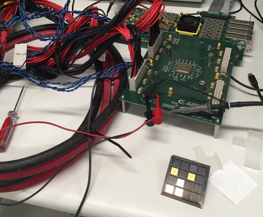
Much of the time spent during algorithm exploration involves running a wide set of parameters through essentially the same algorithm. Plextek came up with a methodology that speeds up the process by providing a parameterised FPGA platform early in the process (see the figure). The approach requires the adoption of new high-level design tools, such as Altera’s DSP Builder or Xilinx’s System Generator.
A major portion of time involved in algorithm exploration revolves around running a wide set of parameters through essentially the same algorithm. Plextek’s methodology provides a parameterized FPGA platform early in the process, which saves a significant amount of time.
A key part of the process is jointly describing the algorithm parameters that are likely to change. After they’re defined, the hardware designer can deliver a platform with super-computing power to the scientist’s local machine, one that’s tailored to the algorithm being studied. At this point, the scientist can very quickly explore parameter changes to the algorithm, often being able to explore previously time-prohibitive ideas. As the algorithm matures, some features may need updating. Though modifications to the FPGA may be required, they can be implemented much faster.
A side benefit of this approach is that the final solution, when achieved, is in a hardware form that can be easily scaled across a business. In the past, algorithm exploration may have used a farm of 100 servers, but when rolled out across a business, the server requirements could increase 10- or 100-fold, or even to thousands of machines. With FPGAs, equipment requirements will experience an orders-of-magnitude reduction.
Ultimately, companies that adopt these methodologies will achieve significant cost and power-consumption savings, as well as speed up their algorithm development flows.
Monday, 19 November 2012
A Brain-On-A-Chip
Sounds Interesting !!!!!
The idea is to devise a “micro-environment’’ that mimics the human brain. Researchers hope to study neurodegenerative conditions such as Alzheimer’s disease, strokes and concussions. The eventual goal is to study the effects of drugs and vaccines on the brain.
Draper, a spinoff from the Massachusetts Institute of Technology (MIT), and USF are using embryonic cells from rats, but researchers plan to use human cells in the future. The brain-on-a-chip combines several technologies, including an emerging field called microfluidics.
Microfluidics deals with the control of fluids in devices. Tiny chip-like devices using microfluidics are used in many applications, such as cell sorting and detection, gene analysis, inkjet print heads, lab-on-a-chip units and point-of-care diagnostic tools. Meanwhile, lab-on-a-chip, and a related field, organ-on-a-chip (i.e. brain-on-a-chip), are systems that integrate various functions in a chip-like format. Some, but not all, lab-on-a-chip systems use microfluidics.
Monday, 5 November 2012
Intel's 335 Series SSD reviewed
SSDs have come a long way since Intel released its first, the X25-M, a little more than four years ago. That drive was a revelation, but it wasn't universally faster than the mechanical hard drives of the era. The X25-M was also horrendously expensive; it cost nearly $600 yet offered just 80GB of capacity, which works out to about $7.50 per gigabyte.
My, how things have changed.
Solid-state drives gotten a lot faster in the last few years. They're already pushing up against the throughput ceiling of the 6Gbps Serial ATA interface, leaving mechanical hard drives in the dust. I can't remember the last time we saw an HDD score better than an SSD in one of our performance tests.
More importantly, SSDs have become a lot more affordable. Today, you can get 80GB by spending $100. The sweet spot in the market is the 240-256GB range, where SSDs can be had for around $200—less than a dollar per gigabyte. Rabid competition between drive makers deserves some credit for falling prices, particularly in recent years. Moore's Law is the real driving factor behind the trend, though. The X25-M's NAND chips were built using a 50-nm process, while the new Intel 335 Series uses flash fabricated on a much smaller 20-nm process.
Designed for enthusiasts and DIY system builders, the 335 Series is aimed squarely at the sweet spot in the market with a 240GB model priced at $184. That's just 77 cents per gig, a tenfold reduction in cost in just four years. The price is right, but what about the performance? We've run Intel's latest through our usual gauntlet of tests to see how it stacks up against the most popular SSDs around.
Die shrinkin'
Intel and Micron have been jointly manufacturing flash memory since 2006 under the name IM Flash Technologies. The pair started with 72-nm NAND flash before moving on to the 50-nm chips used in the X25-M. The next fabrication node was 34 nm, which produced the chips used in the second-generation X25-M and the Intel 510 Series. 25-nm NAND found its way into the third-gen X25-M, otherwise known as the 320 Series, in addition to the 330 and 520 Series. Now, the Intel 335 Series has become the first SSD to use IMFT's 20-nm MLC NAND.
Building NAND on finer fabrication nodes allows more transistors to be squeezed into the same unit area. In addition to accommodating more dies per wafer, this shrinkage can allow more capacity per die. The 34-nm NAND used in the Intel 510 Series offered 4GB per die, with each die measuring 172 mm². When IMFT moved to 25-nm production for the 320 Series, the per-die capacity doubled to 8GB, while the die size shrunk slightly to 167 mm².
Two 4GB 34-nm dies, one 8GB 25-nm die, and the new 8GB 20-nm die. Source: Intel
The Intel 335 Series' 20-nm NAND crams 8GB onto a die measuring just 118 mm². That's not the doubling of bit density we enjoyed in the last transition, but it still amounts to a 29% reduction in die size for the same capacity. Based on how those dies fit onto each wafer, Intel says 20-nm production increases the "gigabyte capacity" of its flash fabs by approximately 50%. IMFT has been mass-producing these chips since December of last year.
As NAND processes shrink, the individual cells holding 1s and 0s get closer together. Closer proximity can increase the interference between the cells, which can degrade both the performance and the endurance of the NAND. Intel's solution to this problem is a planar cell structure with a floating, high-k/metal gate stack. This advanced cell design is purportedly the first of its kind in the flash industry, and Intel claims it delivers performance and reliability comparable to IMFT's 25-nm NAND. Indeed, Intel's performance and endurance specifications for the 335 Series 240GB exactly match those of its 25-nm sibling in the 330 Series.
Intel says the 335 Series 240GB can push sequential read and write speeds of 500 and 450MB/s, respectively. 4KB random read/write IOps are pegged at 42,000/52,000. Thanks to the lower power consumption of its 20-nm flash, the new drive should be able to hit those targets while consuming less power than its predecessor. The 335 Series is rated for power consumption of 275 mW at idle and 350 mW when active, less than half the 600/850 mW ratings of its 25-nm counterpart.
On the endurance front, Intel's new hotness can supposedly withstand 20GB of writes per day for three years, just like the 330 Series. As one might expect, the drive is covered by a three-year warranty. Intel reserves its five-year SSD warranties for the 320 and 520 Series, whose high-endurance NAND is cherry-picked off the standard 25-nm production line. I suspect it will take Intel some time to bin enough higher-grade, 20-nm NAND to fuel upgrades to those other models.
Our performance results will illustrate how the 335 Series compares up to those other Intel SSDs. Expect the 320 Series to be much slower due to its 3Gbps Serial ATA interface. That drive's Intel flash controller can trace its roots back to the original X25-M, so the design is a little long in the tooth. The 520 Series, however, has a 6Gbps interface and higher performance specifications than the 335 Series. The two are based on the same SandForce controller silicon, though.
Monday, 3 September 2012
Intel Chips Will Support Wireless Charging by 2014
Earlier this month it was rumored that Intel was developing a new wireless charging solution it could integrate into the Ultrabook platform. In so doing, it would remove the need to plug your Ultrabook into a power socket directly, instead placing it on a charging pad or at least near a power source.
Intel’s interest in wireless charging has today been confirmed through a new partnership with Integrated Device Technology (IDT). IDT will develop a new integrated transmitter and receiver for Intel, allowing for wireless charging using resonance technology from up to several feet away.
“Our extensive experience in developing the innovative and highly integrated IDTP9030 transmitter and multi-mode IDTP9020 receiver has given IDT a proven leadership position in the wireless power market,” said Arman Naghavi, vice president and general manager of the Analog and Power Division at IDT.
As for when we can expect to see an Intel-branded wireless charging system, IDT is working to provide samples in the first half of 2013, suggesting product integration should happen in time for the major holiday season at the end of next year.
IDT’s Gary Huang has also suggested that eventually wireless charging will expand to power everything on your desktop. So your wireless keyboard, mouse, backup storage device, smartphone, and PC/laptop will all be completely wireless, with each including the necessary components and battery to be charged.
The chipmaker is entering a market where there is already a proposed standard called Qi. Qi has received a wide array of support, including Energizer, Texas Instruments, Verizon, and phone manufacturers including Nokia, Research In Motion, LG, and HTC.
Currently, 88 products are listed by the Wireless Power Consortium as being Qi-compatible, including phones from NTT DoCoMo and HTC.
Intel is not a part of that group, and its wireless charging effort is based ona platform created by IDT is apparently not Qi-compatible. Since Qi is already getting widespread support and Intel’s chips have made it in to very few mobile devices so far, Intel has some work ahead if it is to be a success.
A completely wire-free desk at home sounds great to me, and if this IDT/Intel venture is successful it could be a reality within a year or two.
Monday, 30 July 2012
To 20nm and beyond: ARM targets Intel with TSMC collaboration
The multi-year deal sees ARM tie itself even closer to TSMC, its chip-fabber of choice, as it looks to capitalise on the company's technology to help it maintain a lead over Intel for chip power efficiency.
ARM is ramping up its push to get its highly efficient low-power chips into servers by signing a multi-year agreement with Asian silicon manufacturer TSMC.
Under the deal, the Cambridge-based chip designer has agreed to share technical details with TSMC to help the fabricator make better chips with higher yields, ARM said on Monday. TSMC will also share information, so that ARM can create designs better suited to its manufacturing.
"By working closely with TSMC, we are able to leverage TSMC's ability to quickly ramp volume production of highly integrated SoCs [System-on-a-Chip processors] in advanced silicon process technology," Simon Segars, general manager for ARM's processor and physical IP divisions, said in a statement.
"The ongoing deep collaboration with TSMC provides customers earlier access to FinFET technology to bring high-performance, power-efficient products to market," he added.
The move should keep ARM's chip designs competitive with Intel's in the server market. TSMC's FinFET is akin to Intel's 3D 'tri-gate' method of designing processors with greater densities, which should deliver greater power efficiency and better performance from a cost point of view.
By tweaking its chips to TSMC's process, ARM chips should deliver good yields on the silicon, keeping prices low while maintaining the higher power efficiency that comes with a lower process node.
ARM's chips dominate the mobile device market, but unlike Intel, it doesn't have a brand presence on the end devices. Instead, companies license its designs, go to a manufacturer, and rebrand the chips under their own name. You may not have heard of ARM, but the Apple, Qualcomm and Nvidia chips in mobile devices, as well as Calxeda and Marvell's server chips, are all based to some degree on based on ARM's low-power RISC-architecture processors.
64-bit processors
As part of the new deal, ARM is expecting to work with TSMC on 64-bit processors. It stressed how the 20nm process nodes provided by the fabber will make its server-targeted chips more efficient, potentially cutting datacentre electricity bills.
"This collaboration brings two industry leaders together earlier than ever before to optimise our FinFET process with ARM's 64-bit processors and physical IP," Cliff Hou, vice president of research and development for TSMC, said in the statement. "We can successfully achieve targets for high speed, low voltage and low leakage."
"We can successfully achieve targets for high speed, low voltage and low leakage" — Cliff Hou, TSMC
However, ARM only released its 64-bit chips in October, putting these at least a year and a half away from production, as licensees tweak designs to fit their devices. Right now, there are few ARM-based efforts pitched at the enterprise, aside from HP's Redstone Server Development platform and a try-before-you-buy ARM-based cloud for the OpenStack software.
Production processes
AMD, like ARM, does not operate its own chip fabrication facilities and so must depend on the facilities of others. AMD uses GlobalFoundries, while ARM licensees have tended to use TSMC. However, both TSMC and GlobalFoundries are a bit behind Intel in terms of the level of detail — the process node — they can make their chips to.
Right now, TSMC is still qualifying its 20nm process for certification by suppliers, while Intel has been shipping its 22nm Ivy Bridge processors for several months. Intel has claimed a product roadmap down to 14nm via use of its tri-gate 3D transistor technology, while TSMC is only saying in the ARM statement it will go beyond 20nm, without giving specifics.
Even with this partnership, Intel looks set to maintain its lead in advanced silicon manufacturing.
"By the time TSMC gets FinFET into production - earliest 2014, it's only just ramping 28nm [now] - Intel will be will into its 2nd generation FinFET buildout," Malcolm Penn, chief executive of semiconductor analysts Future Horizons, told ZDNet. This puts Intel "at least three years ahead of TSMC. Global Foundries will be even later."
Intel has noticed ARM's rise and has begun producing its own low-power server chips under the Centerton codename. However, these chips consume 6W compared with ARM's 5W.
At the time of writing, neither ARM nor TSMC had responded to requests for further information. Financial terms, if any, were not disclosed.
Monday, 16 July 2012
MIT engineers Innovates an “Intelligent co-pilot” for cars
IT engineers have developed a semi-autonomous vehicle safety system that takes over if the driver does something stupid.
The system uses an onboard camera and laser rangefinder to identify hazards. An algorithm analyzes the data and identifies safe zones — avoiding, for example, barrels in a field, or other cars on a roadway.
The driver's in charge - until the system recognizes that the vehicle's about to exit a safe zone and takes over.
"The real innovation is enabling the car to share [control] with you," says PhD student Sterling Anderson. "If you want to drive, it’ll just make sure you don’t hit anything."
The team's approach is based on identifying safe zones, or 'homotopies', rather than specific paths of travel. Instead of mapping out individual paths along a roadway, the researchers divide a vehicle’s environment into triangles, with certain 'constrained' triangle edges representing an obstacle or a lane’s boundary.
If a driver looks like crossing a constrained edge — for instance, if he’s fallen asleep at the wheel and is about to run into a barrier — the system takes over, steering the car back into the safe zone.
The system works well in tests, say its designers: in more than 1,200 trials of the system, with , there have only been a few collisions, mostly when glitches in the vehicle’s camera failed to identify an obstacle.
One possible problem with the system, though, is that it could give drivers a false sense of confidence on their own abilities.
Using it, says Anderson, "You’d say, ‘Hey, I pulled this off,’ and you wouldn’t know that the car is changing things behind the scenes to make sure the vehicle remains safe, even if your inputs are not."
He and Iagnemma are now exploring ways to tailor the system to various levels of driving experience.
They're also hoping to pare down the system to identify obstacles using a single cellphone.
"You could stick your cellphone on the dashboard, and it would use the camera, accelerometers and gyro to provide the feedback needed by the system," says Anderson.
"I think we'll find better ways of doing it that will be simpler, cheaper and allow more users access to the technology."
-
This is 8-bit microprocessor with 5 instructions. It is based on 8080 architecture. This architecture called SAP for Simple-As-Possible comp...
-
Q1: What is UVM? What is the advantage of UVM? Ans: UVM (Universal Verification Methodology) is a standardized methodology for verify...
-
There are some differences between UDIMMs and RDIMMs that are important in choosing the best options for memory performance. First, let’s ta...
-
Up/down counter circuits are very useful devices. A common application is in machine motion control, where devices called rotary shaft encod...
-
A small RISC CPU (written in VHDL) that is compatible with the 12 bit opcode PIC family. Single cycle operation normally, two cycles when th...