Featured post

Top 5 books to refer for a VHDL beginner

VHDL (VHSIC-HDL, Very High-Speed Integrated Circuit Hardware Description Language) is a hardware description language used in electronic des...

Wednesday, 9 September 2015

UVM Interview Questions - 2

Q16: Is uvm is independent of systemverilog ?

Ans: UVM is a methodology based on SystemVerilog language and is not a language on its own.  It is a standardized methodology that defines several best practices in verification to enable  efficiency in terms of reuse and is also currently part of IEEE 1800.2  working group.

Q17: What are the benefits of using UVM?

Ans: Some of the benefits of using UVM are :

  • Modularity and Reusability – The methodology is designed as modular components (Driver, Sequencer, Agents , env etc) which enables reusing components across unit level to multi-unit or chip level verification as well as across projects.
  • Separating Tests from Testbenches – Tests in terms of stimulus/sequencers are kept separate from the actual testbench hierarchy and hence there can be reuse of stimulus across different units or across projects
  • Simulator independent – The base class library and the methodology is supported by all simulators and hence there is no dependence on any specific simulator
  • Better control on Stimulus generation – Sequence methodology gives good control on stimulus generation. There are several ways in which sequences can be developed which includes randomization, layered sequences, virtual sequences etc which provides a good control and rich stimulus generation capability.
  • Easy configuration – Config mechanisms simplify configuration of objects with deep hierarchy. The configuration mechanism helps in easily configuring different testbench components based on which verification environment uses it and without worrying about how deep any component is in testbench hierarchy
  • Factory mechanism – Factory mechanisms simplifies modification of components easily. Creating each components using factory enables them to be overridden in different tests or environments without changing underlying code base.


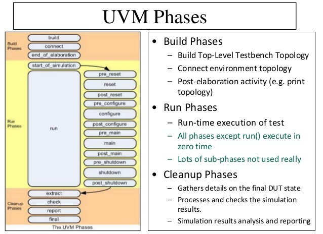
Q18: Can we have user defined phase in UVM?

Ans: In addition to the predefined phases available in uvm , the user has the option to add his own phase to a component. This is typically done by extending the uvm_phase class the constructor needs to call super.new which has three arguments
  • Name of the phase task or function
  • Top down or bottom up phase
  • Task or function


The call_task  or call_func and get_type_name need to be implemented to complete the addition of new phase.
Below is a simple example 

Example
class custom_phase extends uvm_phase;
   function new();
      super.new(“custom”,1,1);
   endfunction

   task call_task  ( uvm_component parent);
     my_comp_type comp;
     if ( $cast(comp,parent) )
             comp.custom_phase();
   endtask

   virtual function string get_type_name();
      return “custom”;
   endfunction
endclass


Q19: What is uvm RAL model ? why it is required ?

Ans: In a verification context, a register model (or register abstraction layer) is a set of classes that model the memory mapped behavior of registers and memories in the DUT in order to facilitate stimulus generation and functional checking (and optionally some aspects of functional coverage). The UVM provides a set of base classes that can be extended to implement comprehensive register modeling capabilities.

Q20: What is the difference between new() and create?

Ans: We all know about new() method that is use to allocate memory to an object instance. In UVM (and OVM), the create() method causes an object instance to be created from the factory. This allows you to use factory overrides to replace the desired object with an object of a different type without having to recode.

<< PREVIOUS      NEXT >>

UVM Interview Questions

Q1: What is UVM? What is the advantage of UVM?

Ans: UVM (Universal Verification Methodology) is a standardized methodology for verifying the both complex & simple digital design in simple way.

UVM Features:
  • First methodology & second collection of class libraries for Automation
  • Reusability through testbench
  • Plug & Play of verification IPs
  • Generic Testbench Development
  • Vendor & Simulator Independent
  • Smart Testbench i.e. generate legal stimulus as from pre-planned coverage plan
  • Support CDV –Coverage Driven Verification
  • Support CRV –Constraint Random Verification
  • UVM standardized under the Accellera System Initiative
  • Register modeling

Q2: UVM derived from which language?

Ans: Here is the detailed connection between SV, UVM, OVM and other methodologies. 


Q3. What is the difference between uvm_component and uvm_object?
                       OR
We already have uvm_object, why do we need uvm_component which is actually derived class of uvm_object?

Ans: 
uvm_component:
  • Quasi Static Entity (after build phase it is available throughout the simulation)
  • Always tied to a given hardware(DUT Interface) Or a TLM port
  • Having phasing mechanism for control the behavior of simulation
  • Configuration Component Topology

uvm_object:
  • Dynamic Entity (create when needed, transfer from one component to other & then dereference)
  • Not tied to a given hardware or any TLM port
  • Not phasing mechanism 

Q4: Why phasing is used? What are the different phases in uvm?

Ans: UVM Phases is used to control the behavior of simulation in a systematic way & execute in a sequential ordered to avoid race condition. This could also be done in system verilog but manually.
  1. List of UVM Phases:
  2. buid_phase
  3. connect_phase
  4. end_of_elaboration_phase
  5. start_of_simulation_phase       
  6. run _phase  (task)
    Sub Phases of Reset Phase:
    pre_reset_phase
    reset_phase
    post_reset_phase
    pre_configure_phase
    configure_phase
    post_configure_phase
    pre_main_phase
    main_phase
    post_main_phase
    pre_shutdown_phase
    shutdown_phase
    post_shutdown_phase
  7. extract_phase
  8. check_phase
  9. report_phase
Below figure makes it more clear


Q5: Which uvm phase is top - down , bottom – up & parallel?

Ans: Only build phase is a top-down & other phases are bottom-up except run phase which is parallel. The build phase works top-down since the testbench hierarchy may be configure so we need to build the branches before leafs

Q6: Why build phase is top – down & connect phase is bottom – up?

Ans: The connect phase is intended to be used for making TLM connections between components, which is why it occur after build phase. It work bottom-up so that its got the correct implementation all the way up the design hierarchy, if worked top-down this would be not possible

Q7: Which phase is function & which phase is task?

Ans: Only run phase is a task (time consuming phase) & other phases are functions (non-blocking)

Q8: Which phase takes more time and why?

Ans: As previously said the run phase is implemented as task and remaining all are function. run phase will get executed from start of simulation to till the end of simulation. run phase is time consuming, where the testcase is running.

Q9: How uvm phases initiate?

Ans: UVM phases initiate by calling run_test(“test1”) in top module. When run_test() method call, it first create the object of test top & then call all phases.

Q10: How test cases run from simulation command line?

Ans: In top module write run_test(); i.e. Don't give anything in argument.
Then in command line : +UVM_TESTNAME=testname

Wednesday, 2 September 2015

Intel's Skylarke Processors for PCs, Tablets and Servers

Intel is launching a full portfolio of "Skylake" processors that company officials expect will combine with Microsoft's Windows 10 operating system to help jump start a stagnant global PC market.

Executives with the chip maker for more than a year have been talking about the 14-nanometer Skylake architecture and the advanced features that are contained within it, touching on everything from graphics and imaging to security, memory, performance and wireless connectivity. In early August, Intel rolled out two Skylake chips—the Core i7-6700K and i5-6600K desktop processors—for gaming machines, and later in the month officials gave out a few more details during the Intel Developer Forum (IDF).

While Intel Corp. is going to release its code-named “Skylake” processors a little later than expected, the company keeps the plan to introduce its new micro-architecture for virtually all segments of the market continuum this year. Intel will roll-out “Skylake” central processing units for tablets, 2-in-1s, personal computers and servers this year, the chip giant confirmed this week.

“When I look at the range of what Skylake’s able to deliver from the Core M level all up to the i7 and Xeon, it’s just going to be a fantastic product,” said Intel CEO Brian Krzanich, in an interview with the IDG News Service at Mobile World Congress in Barcelona.

Intel ran into problems with production of its code-named “Broadwell” processors using 14nm manufacturing technology last year. Due to insufficient yields, the world’s largest maker of microprocessors had to delay introduction of its latest chips by about a year. However, since “Skylake” brings a lot of innovations, Intel did not want to delay it significantly. As a result, “Broadwell” products will have a relatively short lifecycle.

Intel will introduce the first “Skylake” processors in the form of dual-core Core M chips in the third quarter of this calendar year. The CPUs will power high-performance tablets, hybrid 2-in-1 personal computers and ultra-thin notebooks. It is expected that many mobile devices powered by Intel Core M “Skylake” will support Rezence wireless charging and WiGig short-range transmission technology.

In late Q3 or early Q4 the Santa Clara, California-based chip designer will introduce its first Core i3, Core i5 and Core i7 chips featuring “Skylake” micro-architecture for mainstream personal computers, including desktops and laptops. The lineup is projected to include chips with unlocked multiplier designed for enthusiast-class desktop PCs. Systems featuring the new “Skylake” processors will have improved storage performance thanks to native support of SATA Express. In addition, many “Skylake”-powered PCs will use DDR4 memory and support a variety of other innovations.


Intel also plans to introduce Xeon processors with “Skylake” cores for uniprocessor servers later this year. While there are plans to bring “Skylake” architecture to Xeon chips for dual-processor and multi-processor servers, Intel yet has to outline exact plans concerning the move.

Intel “Skylake” processors will be made using 14nm process technology and will feature a brand new micro-architecture that is designed to improve performance and power efficiency of central processing units. Unfortunately, not all “Skylake” processors will support 512-bit AVX 3.2 instructions, according to unofficial information.

Friday, 21 August 2015

Resistive Memory - ReRam

ReRam_Crossbar-Feature_vlsiencyclopedia

The memory tech that will eventually replace NAND flash, finally in market

What is ReRam?

ReRam is Resistive random-access memory (RRAM or ReRAM) is a type of non-volatile (NV) random-access (RAM) computer memory that works by changing the resistance across a dielectric solid-state material often referred to as a memristor. The biggest advantage of ReRAM technology is its good compatibility with CMOS technologies.

It is under development by a number of companies, and some have already patented their own versions of the technology. The memory operates by changing the resistance of special dielectric material called a memresistor (memory resistor) whose resistance varies depending on the applied voltage.

What makes ReRam?

From the viewpoint of the material choice, the advantage of ReRAM is evident. It is possible to fabricate MOM structures easily by using the oxides widely used in the current semiconductor technologies. Low-current ReRAM operation was reported in the CuOx-based MOM structure. The CuOx layer was grown by the thermal oxidation of the 0.18-μm Cu. NiO and CoO are being intensively studied as oxide materials for ReRAM, and these transition metal elements are also used in metal silicides employed as gate materials. Recently, the good scaling feasibility of ReRAM was demonstrated in an HfOx-based memory with a cell size of 30 nm. The devices in a 1-kbit array exhibited a high device yield (~100%) and robust cycling endurance (>106) with a pulse width of 40 ns. The memory cell consisted of a TiN/Ti/HfOx/TiN structure. Here, the Ti overlayer played the role of oxygen gettering for better ReRAM operation. The gettering effect has already been investigated in HfOx as a high-k material for the gate dielectric films in CMOS devices. The academic and technological knowledge about high-k materials will be very useful in the design of the stacking structure for a ReRAM device.

How ReRam Works?

RRAM is the result of a new kind of dielectric material which is not permanently damaged and fails when dielectric breakdown occurs; for a memresistor, the dielectric breakdown is temporary and reversible. When voltage is deliberately applied to a memresistor, microscopic conductive paths called filaments are created in the material. The filaments are caused by phenomena like metal migration or even physical defects. Filaments can be broken and reversed by applying different external voltages. It is this creation and destruction of filaments in large quantities that allows for storage of digital data. Materials that have memresistor characteristics include oxides of titanium and nickel, some electrolytes, semiconductor materials, and even a few organic compounds have been tested to have these characteristics.

The principal advantage of RRAM over other non-volatile technology is high switching speed. Because of the thinness of the memresistors, it has a great potential for high storage density, greater read and write speeds, lower power usage, and cheaper cost than flash memory. Flash memory cannot continue to scale because of the limits of the materials, so RRAM will soon replace flash memory.

Monday, 29 June 2015

Difference between simulation and emulation

Car_racing_simulator_-_SBR_Racing,_Construma,_2015.04.17A simulation is a system that behaves similar to something else, but is implemented in an entirely different way. It provides the basic behaviour of a system but may not necessarily abide by all of the rules of the system being simulated. It is there to give you an idea about how something works.

Think of a flight simulator as an example. It looks and feels like you are flying an airplane, but you are completely disconnected from the reality of flying the plane, and you can bend or break those rules as you see fit. E.g.; Fly an Airbus A380 upside down between London and Sydney without breaking it.

An emulation is a system that behaves exactly like something else, and abides by all of the rules of the system being emulated. It’s like duplicating every aspect of the original device’s behaviour. It is effectively a complete replication of another system, right down to being binary compatible with the emulated system's inputs and outputs, but operating in a different environment to the environment of the original emulated system. The rules are fixed, and cannot be changed or the system fails.

Today hardware emulation has become an very popular tool for verification because of following reasons:

In the past few years, the emulation user community has expanded exponentially by the addition of software developers to the traditional base of hardware designers and verification engineers. 

Also, uses of hardware emulation have multiplied because of its versatility as a resource for debugging both the hardware and software of complex system-on-chip (SoC) designs. Hardware emulation is the only verification tool that can be deployed in more than one mode. In fact, it can be used in four main modes, some of which can be combined for added versatility. Because of this resourcefulness, hardware emulation can be used to achieve several verification objectives.

Following are the deployment modes for hardware emulator. These are characterized by type of stimulus applied to DUT:

  • In Circuit Emulation (ICE) : This was considered to be the traditional method when hardware emulation was deployed. In this case, the DUT is mapped inside the emulator and connected in in-circuit emulation (ICE) mode to the target system in place of a chip or processor for debug prior to silicon availability.
  • Transaction Based Acceleration (TBX) : Transaction-based emulation moves verification up a level of abstraction from the register transfer level (RTL), improving performance and debug productivity. It’s gaining popularity over the ICE mode because the physical target system is replaced by a virtual target system using a hardware verification language (HVL) such as
    SystemVerilog, SystemC, or C++.
  • Simulation Testbench Acceleration : In this mode, an RTL testbench drives the DUT in the emulator via a programmable logic interface (PLI). In general, this is the slowest performance mode, but it has some advantages, such as the fact that it does not require changes to the testbench.
  • Embeded Software Acceleration : In this mode, the software code is executed on the DUT processor mapped inside the emulator. This is the fastest performance mode, making it the choice for processing billions of verification cycles necessary to boot an operating system.

It is possible to mix some of the above modes, such as processing embedded software together with a virtual testbench driving the DUT via verification IP or even in ICE mode.

Wednesday, 13 May 2015

IEEE Standards

vlsi-ieee802IEEE 802 refers to a family of IEEE standards dealing with local area networks and metropolitan area networks.

More specifically, the IEEE 802 standards are restricted to networks carrying variable-size packets. By contrast, in cell relay networks data is transmitted in short, uniformly sized units called cells. Isochronous networks, where data is transmitted as a steady stream of octets, or groups of octets, at regular time intervals, are also out of the scope of this standard. The number 802 was simply the next free number IEEE could assign, though “802” is sometimes associated with the date the first meeting was held — February 1980.

The services and protocols specified in IEEE 802 map to the lower two layers (Data Link and Physical) of the seven-layer OSI networking reference model. In fact, IEEE 802 splits the OSI Data Link Layer into two sub-layers named Logical Link Control (LLC) and Media Access Control (MAC), so that the layers can be listed like this:

  • Data link layer
  • LLC Sublayer
  • MAC Sublayer
  • Physical layer

The IEEE 802 family of standards is maintained by the IEEE 802 LAN/MAN Standards Committee (LMSC). The most widely used standards are for the Ethernet family, Token Ring, Wireless LAN, Bridging and Virtual Bridged LANs. An individual Working Group provides the focus for each area.

IEEE developed a set of 802 network standards. They include:

  • IEEE 802.1: Standards related to network management.
  • IEEE 802.2: General standard for the data link layer in the OSI Reference Model. The IEEE divides this layer into two sub-layers -- the logical link control (LLC) layer and the media access control (MAC) layer. The MAC layer varies for different network types and is defined by standards IEEE 802.3 through IEEE 802.5.
  • IEEE 802.3: Defines the MAC layer for bus networks that use CSMA/CD. This is the basis of the Ethernet standard.
  • IEEE 802.4: Defines the MAC layer for bus networks that use a token-passing mechanism (token bus networks).
  • IEEE 802.5: Defines the MAC layer for token-ring networks.
  • IEEE 802.6: Standard for Metropolitan Area Networks (MANs).

Tuesday, 12 May 2015

Ethernet–Introduction

VLSI_ETHERNETIn today's business world, reliable and efficient access to information has become an important asset in the quest to achieve a competitive advantage. File cabinets and mountains of papers have given way to computers that store and manage information electronically.

Computer networking technologies are the glue that binds these elements together. Networking allows one computer to send information to and receive information from another. We can classify network technologies as belonging to one of two basic groups. Local area network (LAN) technologies connect many devices that are relatively close to each other, usually in the same building. The library terminals that display book information would connect over a local area network. Wide area network (WAN) technologies connect a smaller number of devices that can be many kilometers apart.

In comparison to WANs, LANs are faster and more reliable, but improvements in technology continue to blur the line of demarcation. Fiber optic cables have allowed LAN
technologies to connect devices tens of kilometers apart, while at the same time greatly
improving the speed and reliability of WANs.

Read More >>