Featured post

Top 5 books to refer for a VHDL beginner

VHDL (VHSIC-HDL, Very High-Speed Integrated Circuit Hardware Description Language) is a hardware description language used in electronic des...

Showing posts with label tricks. Show all posts

Monday, 25 March 2013

Use SystemVerilog for coverage metrics

The design-and-verification industry is at the intersection of two important trends in the design and verification of SOC (system-on-chip) devices: the adoption of SystemVerilog HDVL (hardware-description and -verification language) and the increasingly critical role for coverage metrics. The interest in System Verilog is understandable; this IEEE-standard language has the features for RTL (register-transfer-level) design, high-level modeling, testbench creation, and assertion specification (Reference).

SystemVerilog also provides constructs for design-and-verification engineers to specify functional coverage points—conditions that designers must exercise for complete verification of the design. Designers increasingly use functional coverage to supplement traditional code coverage. The primary driver for this evolution is the widespread use of constrained-random-stimulus generation.

Traditional verification plans typically include a list of design features or tests that verify features and test status. This approach has worked well with handwritten, directed tests because of the clear correspondence between features and tests. However, verification consists of writing and running each test in simulation, perhaps after turning on some code coverage to help identify features you may have missed in the plan.

Constrained-random-stimulus generation requires a different approach, in which each automatically generated test can exercise many features and parts of the design. A modern verification plan lists features, functional coverage points for the features, and coverage status. You gauge verification closure by the number of coverage points you exercise rather than the number of tests you complete.

SystemVerilog provides all the features necessary to develop both handwritten tests and constrained-random testbenches and to track progress toward closure. Most simulators have built-in code coverage for the new design constructs that SystemVerilog introduces. Thus, code-coverage metrics are available for designs taking advantage of the language's advanced RTL features.

SystemVerilog provides several powerful specification methods for functional coverage. The first is cover property, which is part of the SVA (SystemVerilog Assertions) subset of the language. SVA's assertion features, including temporal sequences, are also available for functional coverage.
For example,

MiniMuM and MaxiMuM response
minimum_response: cover property (@(posedge clk)
(req ##1 ack ));
maximum_response: cover property (@(posedge clk)
(req ##5 ack ));

Above example ensures that the simulator exercises the two extremes—one and five cycles—of a request-acknowledge handshake. Both simulators and many formal-analysis tools support the cover-property construct. If formal analysis can prove that a coverage point is unreachable, a design bug may be blocking important functions from being exercised. If formal analysis instead provides a trace showing how to reach a coverage point, this trace can provide a good hint on how to write or generate a test.

Beyond individual coverage properties, you sometimes must track ranges of values. SystemVerilog provides the cover-group construct, which is not part of SVA, to perform this function.
For example,

PayLoad sizes of incoming Packets
minimum_response: cover property (@(posedge clk)
(req ##1 ack ));
maximum_response: cover property (@(posedge clk)
(req ##5 ack ));
covergroup payloads_seen (@(packet_received);
coverpoint payload_size {
bins empty = { 0 };
bins minimum = { 1 };
bins maximum= { 1023 };
bins others = default; }
endgroup : payloads_seen

Above example tracks the payload sizes of incoming packets on a network interface and ensures the coverage of corner cases of empty, minimum, and maximum payloads. SystemVerilog also provides the cross construct to measure cross-coverage between two coverage points. This feature allows the tracking of combinations of coverage metrics.
For example,

EnumEratEd typE for four packEt cLassEs

enum { read, write, atomic, ctrl } packet_class;
covergroup packets_seen (@(packet_received);
coverpoint payload_size {
bins empty = { 0 };
bins minimum = { 1 };
bins maximum= { 1023 };
bins others = default; }
coverpoint packet_class;
cross payload_size, packet_class;
endgroup : packets_seen

Above example specifies an enumerated type for four packet classes for the network interface, adds a cover point to track the packet classes, and crosses the packet types with the payload sizes.

Ultimately, the SOC-tapeout decision must take into account all coverage metrics. Although functional coverage is the primary method, code coverage has value as a backup to identify areas of the design with no functional coverage due to an incomplete verification plan. The project team needs to merge together code- and functional-coverage results to assess verification progress and help determine verification closure. Coverage is critical for modern, constrained-random verification. Without effective metrics, no reliable way exists to gauge status and manage progress. In addition to its other features and benefits, SystemVerilog provides support for functional coverage. By including coverage in the verification plan from the start of the project and taking advantage of SystemVerilog, the SOC team can employ a complete plan-to-closure methodology that greatly increases the chances for a successful product.

Thursday, 21 February 2013

How to read an NGC netlist file

For the occasions that you find yourself with a netlist file and you don’t know where it came from or what version it is, etc. this post is about how you can interpret the netlist file (ie. convert it into something readable).

Today I found myself with two netlists and I needed to know if they were the same. Yes of course you can try comparing the two files with a program such as Beyond Compare, but if the netlists were compiled on separate dates, you will have trouble recognizing this from the raw binary data. The best thing to do in this case is to convert the netlists to EDIF files, a readable, text file version of the netlist. Another option is to convert the netlists into VHDL or Verilog code. Here is how you can do this:

To convert a netlist (.ngc) to an EDIF file (.edf)

  1. Get a command window open by typing “cmd” in the Start->Run menu option in Windows. If you use Linux, open up a terminal window.
  2. Use the “cd” command to move to the folder in which you keep your netlist.
  3. Type “ngc2edif infilename.ngc outfilename.edf” where infilename and outfilename correspond to the input and output filenames respectively.
  4. Open the .edf file with any text editor to view the netlist.

To reverse engineer a netlist with ISE versions older than 6.1i

  1. Convert the netlist to an EDIF file using the above instructions.
  2. Type “edif2ngd filename.edf filename.ngd” to convert the EDIF file into an NGD file (Xilinx Native Generic Database file).
  3. To convert the netlist into VHDL type “ngd2vhdl filename.ngd filename.vhd“.
  4. To convert the netlist into Verilog type “ngd2ver filename.ngd filename.v“.

To reverse engineer a netlist with ISE versions 6.1i and up

  1. To convert the netlist into VHDL type “netgen -ofmt vhdl filename.ngc“. Netgen will create a filename.vhd file.
  2. To convert the netlist into Verilog type “netgen -ofmt verilog filename.ngc“. Netgen will create a filename.v file.

Now you should have all the tools you need to read an NGC netlist file.

Get free daily email updates!

Follow us!

Sunday, 14 October 2012

Cyclic Redundancy Check - CRC

crc-polynom-generationCRC Example 

Error detection is an important part of communication systems when there is a chance of data getting corrupted. Whether it’s a piece of stored code or a data transmission, you can add a piece of redundant information to validate the data and protect it against corruption. Cyclic redundancy checking is a robust error-checking algorithm, which is commonly used to detect errors either in data transmission or data storage. In this multipart article we explain a few basic principles.

Modulo two arithmetic is simple single-bit binary arithmetic with all carries or borrows ignored. Each digit is considered independently. This article talks about how modulo two addition is equivalent to modulo two subtraction, and can be performed using an exclusive OR operation followed by a brief on Polynomial division where remainder forms the CRC checksum.

For example, we can add two binary numbers X and Y as follows:

10101001 (X) + 00111010 (Y) = 10010011 (Z)

From this example the modulo two addition is equivalent to an exclusive OR operation. What is less obvious is that modulo two subtraction gives the same results as an addition.

From the previous example let’s add X and Z:
10101001 (X) + 10010011 (Z) = 00111010 (Y)

In our previous example we have seen how X + Y = Z therefore Y = Z – X, but the example above shows that Z+X = Y also, hence modulo two addition is equivalent to modulo two subtraction, and can be performed using an exclusive OR operation.

In integer division dividing A by B will result in a quotient Q, and a remainder R. Polynomial division is similar except that when A and B are polynomials, the remainder is a polynomial, whose degree is less than B.

The key point here is that any change to the polynomial A causes a change to the remainder R. This behavior forms the basis of the cyclic redundancy checking.

If we consider a polynomial, whose coefficients are zeros and ones (modulo two), this polynomial can be easily represented by its coefficients as binary powers of two.

In terms of cyclic redundancy calculations, the polynomial A would be the binary message string or data and polynomial B would be the generator polynomial. The remainder R would be the cyclic redundancy checksum. If the data changed or became corrupt, then a different remainder would be calculated.

Although the algorithm for cyclic redundancy calculations looks complicated, it only involves shifting and exclusive OR operations. Using modulo two arithmetic, division is just a shift operation and subtraction is an exclusive OR operation.

Cyclic redundancy calculations can therefore be efficiently implemented in hardware, using a shift register modified with XOR gates. The shift register should have the same number of bits as the degree of the generator polynomial and an XOR gate at each bit, where the generator polynomial coefficient is one.

Augmentation is a technique used to produce a null CRC result, while preserving both the original data and the CRC checksum. In communication systems using cyclic redundancy checking, it would be desirable to obtain a null CRC result for each transmission, as the simplified verification will help to speed up the data handling.

Traditionally, a null CRC result is generated by adding the cyclic redundancy checksum to the data, and calculating the CRC on the new data. While this simplifies the verification, it has the unfortunate side effect of changing the data. Any node receiving the data+CRC result will be able to verify that no corruption has occurred, but will be unable to extract the original data, because the checksum is not known. This can be overcome by transmitting the checksum along with the modified data, but any data-handling advantage gained in the verification process is offset by the additional steps needed to recover the original data.

Augmentation allows the data to be transmitted along with its checksum, and still obtain a null CRC result. As explained before when obtain a null CRC result, the data changes, when the checksum is added. Augmentation avoids this by shifting the data left or augmenting it with a number of zeros, equivalent to the degree of the generator polynomial. When the CRC result for the shifted data is added, both the original data and the checksum are preserved.

In this example, our generator polynomial (x3 + x2 + 1 or 1101) is of degree 3, so the data (0xD6B5) is shifted to the left by three places or augmented by three zeros.
0xD6B5 = 1101011010110101 becomes 0x6B5A8 = 1101011010110101000.

Note that the original data is still present within the augmented data.

0x6B5A8 = 1101011010110101000
Data = D6B5 Augmentation = 000

Calculating the CRC result for the augmented data (0x6B5A8) using our generator polynomial (1101), gives a remainder of 101 (degree 2). If we add this to the augmented data, we get:

0x6B5A8 + 0b101 = 1101011010110101000 + 101
= 1101011010110101101
= 0x6B5AD

As discussed before, calculating the cyclic redundancy checksum for 0x6B5AD will result in a null checksum, simplifying the verification. What is less apparent is that the original data is still preserved intact.

0x6B5AD = 1101011010110101101
Data = D6B5 CRC = 101

The degree of the remainder or cyclic redundancy checksum is always less than the degree of the generator polynomial. By augmenting the data with a number of zeros equivalent to the degree of the generator polynomial, we ensure that the addition of the checksum does not affect the augmented data.

In any communications system using cyclic redundancy checking, the same generator polynomial will be used by both transmitting and receiving nodes to generate checksums and verify data. As the receiving node knows the degree of the generator polynomial, it is a simple task for it to verify the transmission by calculating the checksum and testing for zero, and then extract the data by discarding the last three bits.

Thus augmentation preserves the data, while allowing a null cyclic redundancy checksum for faster verification and data handling.

Get free daily email updates!

Follow us!

Monday, 10 September 2012

Intel Is Cooling Entire Servers By Submerging Them in Oil

originalAir cooled computers are for wimps. But while the idea of keeping temperatures in check using water might be a step in the right direction, Intel is doing something even more radical: it's dunking entire servers—the whole lot—into oil to keep them chill.

Don't panic, though: they're using mineral oil, which doesn't conduct electricity. It's a pretty wacky idea, but it seems to be working. After a year of testing with Green Revolution Cooling, Intel has observed some of the best efficiency ratings it's ever seen. Probably most impressive is that immersion in the oil doesn't seem to affect hardware reliability.

All up, it's extremely promising: completely immersing components in liquid means you can pack components in more tightly as the cooling is so much more efficient. For now, though, it's probably best to avoid filling your computer case with liquid of any kind.


Get free daily email updates!

Follow us!

Thursday, 6 September 2012

Choosing FPGA or DSP for your Application


FPGA or DSP - The Two Solutions

The DSP is a specialised microprocessor - typically programmed in C, perhaps with assembly code for performance. It is well suited to extremely complex maths-intensive tasks, with conditional processing. It is limited in performance by the clock rate, and the number of useful operations it can do per clock. As an example, a TMS320C6201 has two multipliers and a 200MHz clock – so can achieve 400M multiplies per second.

In contrast, an FPGA is an uncommitted "sea of gates". The device is programmed by connecting the gates together to form multipliers, registers, adders and so forth. Using the Xilinx Core Generator this can be done at a block-diagram level. Many blocks can be very high level – ranging from a single gate to an FIR or FFT. Their performance is limited by the number of gates they have and the clock rate. Recent FPGAs have included Multipliers especially for performing DSP tasks more efficiently. – For example, a 1M-gate Virtex-II™ device has 40 multipliers that can operate at more than 100MHz. In comparison with the DSP this gives 4000M multiplies per second.


Where They Excel


When sample rates grow above a few Mhz, a DSP has to work very hard to transfer the data without any loss. This is because the processor must use shared resources like memory busses, or even the processor core which can be prevented from taking interrupts for some time. An FPGA on the other hand dedicates logic for receiving the data, so can maintain high rates of I/O.

A DSP is optimised for use of external memory, so a large data set can be used in the processing. FPGAs have a limited amount of internal storage so need to operate on smaller data sets. However FPGA modules with external memory can be used to eliminate this restriction.

A DSP is designed to offer simple re-use of the processing units, for example a multiplier used for calculating an FIR can be re-used by another routine that calculates FFTs. This is much more difficult to achieve in an FPGA, but in general there will be more multipliers available in the FPGA. 

If a major context switch is required, the DSP can implement this by branching to a new part of the program. In contrast, an FPGA needs to build dedicated resources for each configuration. If the configurations are small, then several can exist in the FPGA at the same time. Larger configurations mean the FPGA needs to be reconfigured – a process which can take some time.

The DSP can take a standard C program and run it. This C code can have a high level of branching and decision making – for example, the protocol stacks of communications systems. This is difficult to implement within an FPGA.

Most signal processing systems start life as a block diagram of some sort. Actually translating the block diagram to the FPGA may well be simpler than converting it to C code for the DSP.

Making a Choice

There are a number of elements to the design of most signal processing systems, not least the expertise and background of the engineers working on the project. These all have an impact on the best choice of implementation. In addition, consider the resources available – in many cases, I/O modules have FPGAs on board. Using these with a DSP processor may provide an ideal split.


As a rough guideline, try answering these questions:

  1. What is the sampling rate of this part of the system? If it is more than a few MHz, FPGA is the natural choice.
  2. Is your system already coded in C? If so, a DSP may implement it directly. It may not be the highest performance solution, but it will be quick to develop.
  3. What is the data rate of the system? If it is more than perhaps 20-30Mbyte/second, then FPGA will handle it better.
  4. How many conditional operations are there? If there are none, FPGA is perfect. If there are many, a software implementation may be better.
  5. Does your system use floating point? If so, this is a factor in favour of the programmable DSP. None of the Xilinx cores support floating point today, although you can construct your own.
  6. Are libraries available for what you want to do? Both DSP & FPGA offer libraries for basic building blocks like FIRs or FFTs. However, more complex components may not be available, and this could sway your decision to one approach or the other.

In reality, most systems are made up of many blocks. Some of those blocks are best implemented in FPGA, others in DSP. Lower sampling rates and increased complexity suit the DSP approach; higher sampling rates, especially combined with rigid, repetitive tasks, suit the FPGA.


Some Examples

Here are a few examples of signal processing blocks, along with how we would implement them:

  1. First decimation filter in a digital wireless receiver. Typically, this is a CIC filter, operating at a sample rate of 50-100MHz. A 5-stage CIC has 10 registers & 10 adds, giving an "add rate" of 500-1000MHz.
    At these rates any DSP processor would find it extremely difficult to do anything. However, the CIC has an extremely simple structure, and implementing it in an FPGA would be easy. A sample rate of 100MHz should be achievable, and even the smallest FPGA will have a lot of resource left for further processing.
  2. Communications Protocol Stack – ISDN, IEEE1394 etc; these are complex large pieces of C code, completely unsuitable for the FPGA. However the DSP will implement them easily. Not only that, a single code base can be maintained, allowing the code stack to be implemented on a DSP in one product, or a separate control processor in another; and bringing the opportunity to licence the code stack from a specialist supplier.
  3. Digital radio receiver – baseband processing. Some receiver types would require FFTs for signal acquisition, then matched filters once a signal is acquired. Both blocks can be easily implemented by either approach. However, there is a mode change – from signal acquisition to signal reception.
    It may well be that this is better suited to the DSP, as the FPGA would need to implement both blocks simultaneously. Note that the RF processing is better in an FPGA, so this is likely to be a mixed system.
    (Note – with today’s larger FPGAs, both modes of this system could be included in the FPGA at the same time.)
  4. Image processing. Here, most of the operations on an image are simple and very repetitive – best implemented in an FPGA. However, an imaging pipeline is often used to identify "blobs" or "Regions of Interest" in an object being inspected. These blobs can be of varying sizes, and subsequent processing tends to be more complex. The algorithms used are often adaptive, depending on what the blob turns out to be… so a DSP-based approach may be better for the back end of the imaging pipeline.

Summary

FPGA and DSP represent two very different approaches to signal processing – each good at different things. There are many high sampling rate applications that an FPGA does easily, while the DSP could not. Equally, there are many complex software problems that the FPGA cannot address.

Tuesday, 24 July 2012

Editing your FPGA source

I noted that in a recent poll of FPGA developers, emacs was far and away the most popular VHDL and Verilog editor. There are a few reasons for this – namely, emacs comes with packages for editing your HDL of choice. For those of us not wanting to install (and learn) the emacs operating system, I got Notepad++ to work with these packages.

Notepad++ already has VHDL and Verilog highlighting along with other advanced text editor features, but I wanted templates, automated declarations and beautification. To do this, he used the FingerText to store code as snippets and call them up at the wave of a finger.

As I writes his code, the component declarations constantly need to be updated, and with the help of a Perl script I can update them with the click of a hotkey. Beautification is a harder nut to crack, as Notepad++ doesn’t even have a VHDL or Verilog beautifier plugin. This was accomplished by installing emacs and running the beautification process as a batch script. Nobody can have it all, but we’re thinking that this method of getting away from emacs is pretty neat.

Monday, 16 January 2012

Shared Variable in VHDL

How to use a single variable in more than one process…!!

VHDL87 limited the scope of the variable to the process in which it was declared. Signals were the only means of communication between processes, but signal assignments require an advance in either delta time or simulation time.

VHDL '93 introduced shared variables which are available to more than one process. Like ordinary VHDL variables, their assignments take effect immediately. However, caution must be exercised when using shared variables because multiple processes making assignments to the same shared variable can lead to unpredictable behavior if the assignments are made concurrently. The VHDL ‘93 standard does not define the value of a shared variable it two or more processes make assignments in the same simulation cycle.

The syntax of the shared variable is similar to that of the normal variable. However, the keyword SHARED is placed in front of VARIABLE in the declaration

Example:

Architecture SV_example of example is
      shared variable status_signal : bit;
begin
     p1 : process (Clock,In1)
     begin
          if(status_signal) then
          ...
          end if;
          status_signal :='0';
     end process;

     p2 : process (Clock,In2)
     begin
          if(!(status_signal)) then
          ....
          end if;
          status_signal:='1';
     end process p2;

end SV_example;

Above example shows the use of shared variable in more than one process.

Friday, 23 December 2011

Compiling Xilinx library for ModelSim simulator

It was all running cool with VHDL but when i tried to do post Place and Route simulation using SDF file of my design i stuck with following errors:

# ** Error: (vsim-SDF-3250) mips_struct.sdf(18): Failed to find INSTANCE '/top/dut/U1262'.
# ** Error: (vsim-SDF-3250) mips_struct.sdf(19): Failed to find INSTANCE '/top/dut/U1262'.
# ** Error: (vsim-SDF-3250) mips_struct.sdf(20): Failed to find INSTANCE '/top/dut/U1262'.
# ** Error: (vsim-SDF-3250) mips_struct.sdf(21): Failed to find INSTANCE '/top/dut/U1261'.
# ** Error: (vsim-SDF-3250) mips_struct.sdf(22): Failed to find INSTANCE '/top/dut/U1261'

googling a lot i found that i need to compile xilinx libraries and had to map it with ModelSim to get it worked. For this u need to write CompXlib in your TCL window of Xilinx.

CompXLib uses the ModelSim "vmap" command for library mapping. If the ModelSim environment variable is set, then the ".ini" file pointed to by the environment variable is modified. If the variable is not set, a local (in the directory in which CompXLib is run) "modelsim.ini" file contains the library mappings from the "vmap" command issued by CompXLib. If the "modelsim.ini" file is not writeable, the "vmap" command will make a local copy of the "modelsim.ini" file and write the library mappings to this file.

I used the “compxlib” command but still it was not working for me. When i checked my modelsim.ini file I found that the libraries was not mapped so i write below command in the modelsim.ini file and finally i find all compiled xilinx libraries in my library window of modelsim.

UNISIMS_VER = C:\Xilinx\10.1\ISE\verilog\mti_se\unisims_ver
UNIMACRO_VER = C:\Xilinx\10.1\ISE\verilog\mti_se\unimacro_ver
UNI9000_VER = C:\Xilinx\10.1\ISE\verilog\mti_se\uni9000_ver
SIMPRIMS_VER = C:\Xilinx\10.1\ISE\verilog\mti_se\simprims_ver
XILINXCORELIB_VER = C:\Xilinx\10.1\ISE\verilog\mti_se\XilinxCoreLib_ver
SECUREIP = C:\Xilinx\10.1\ISE\vhdl\mti_se\secureip
AIM_VER = C:\Xilinx\10.1\ISE\verilog\mti_se\abel_ver\aim_ver
CPLD_VER = C:\Xilinx\10.1\ISE\verilog\mti_se\cpld_ver
UNISIM = C:\Xilinx\10.1\ISE\vhdl\mti_se\unisim
UNIMACRO = C:\Xilinx\10.1\ISE\vhdl\mti_se\unimacro
SIMPRIM = C:\Xilinx\10.1\ISE\vhdl\mti_se\simprim
XILINXCORELIB = C:\Xilinx\10.1\ISE\vhdl\mti_se\XilinxCoreLib
AIM = C:\Xilinx\10.1\ISE\vhdl\mti_se\abel\aim
PLS = C:\Xilinx\10.1\ISE\vhdl\mti_se\abel\pls
CPLD = C:\Xilinx\10.1\ISE\vhdl\mti_se\cpld

** C:\Xilinx\10.1 is path in my system. Please check paths and make changes accordingly.

alternatively you can also use following commands

compxlib -s mti_se -arch virtex -lib unisim -lib simprim -lib xilinxcorelib -l vhdl -dir C:\Mentor\libraries\xilinx\10.1\ISE_Lib\ -log compxlib.log -w
compxlib -s mti_se -arch virtex2p -lib unisim -lib simprim -lib xilinxcorelib -l vhdl -dir C:\Mentor\libraries\xilinx\10.1\ISE_Lib\ -log compxlib.log -w
compxlib -s mti_se -arch virtex4 -lib unisim -lib simprim -lib xilinxcorelib -l vhdl -dir C:\Mentor\libraries\xilinx\10.1\ISE_Lib\ -log compxlib.log -w
compxlib -s mti_se -arch spartan3 -lib unisim -lib simprim -lib xilinxcorelib -l vhdl -dir C:\Mentor\libraries\xilinx\10.1\ISE_Lib\ -log compxlib.log -w
compxlib -s mti_se -arch virtex5 -lib unisim -lib simprim -lib xilinxcorelib -l vhdl -dir C:\Mentor\libraries\xilinx\10.1\ISE_Lib\ -log compxlib.log –w

**(C:\Mentor\libraries\xilinx\10.1\ISE_Lib\  is my path, you can use your own)

Wednesday, 15 June 2011

Seven steps to a bootable Windows 7 thumb drive

Yesterday i thought to install windows 7 to my pc using a bootable windows 7 thumb drive, but creating a bootable USB drive for windows 7 is very complicated.

There are plenty of great tutorials out there that basically contain the same information as this one, but I thought I’d try to put together a how-to guide that made everything as simple as possible for people who might like the idea of Windows on a thumb drive but aren’t necessarily super comfortable with the actual process.
The only tangible thing you’ll need is a USB thumb drive with at least 4GB of capacity. I found a SanDisk Cruzer Contour worked best, while a Kingston DataTraveler was a bit fidgety at first but worked after a couple of tries.
It’s all pretty easy once you get going, so let’s begin.
Step One: Download Windows 7 Beta

Head over to http://www.microsoft.com/windows/windows-7/beta-download.aspxand jump through all the hoops to begin your download. For the sake of this exercise, we’ll assume that you’ll download the ISO file to your desktop. The download might take a while depending on your connection speed – set aside an hour to be on the safe side. Meanwhile, take a break. You’ve earned it!
Step Two: Download and install WinRAR

I hate guides that make me go download a bunch of software just to accomplish a task, so I apologize for making you do the same thing. I promise this will be the only third-party software that you’ll have to download and install, though, and it’s a great program to have on your computer anyway if you don’t already.
Head over to http://rarsoft.com/download.htm and click on the WinRAR 3.80 link to download the software. Once downloaded, install it.
Step Three: Extract the Windows 7 ISO file

Once Windows 7 Beta has finished downloading, you should see a file on your desktop with a bunch of gobbledygook in the name like “7000.0.081212-1400_client_en-us_Ultimate-GB1CULFRE_EN_DVD” or something cryptic like that. Right-click on that file and choose “Extract to [gobbledygook]” as shown in the above picture. When the smoke has cleared, you’ll have a gobbledygook folder on your desktop. I’ll continue to refer to this folder as “the gobbledygook folder” for the rest of this guide.
Step Four: Format a 4GB USB thumb drive

Head into “Computer” or “My Computer” and locate your USB thumb drive. In this instance, we’re dealing with the F: drive. Right click on the drive and choose “Format…” Then, we want to format the drive using the NTFS file system with the default allocation size, so make sure those two things are selected from the dropdown menus. You can check the Quick Format box, too, if it’s not already checked.
Step Five: The tricky BootSect.exe part

Now we’re going to go back to our extracted “7000.0.081212-1400_client_en-us_Ultimate-GB1CULFRE_EN_DVD” gobbledygook folder and open the “boot” folder, inside which we’ll find a file called “bootsect.exe” that we’ll need to use.
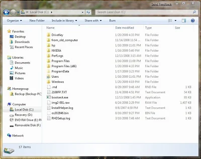
If you’re comfortable navigating folders in DOS, then you can skip this particular step. If you don’t like DOS or haven’t used it much, we’re going to copy this bootsect.exe file into an easy-to-access location. Copy the file (CTRL-C) and then open up “Computer” or “My Computer” and double-click your C: drive.

We’re going to paste (CTRL-V) that “bootsect.exe” file right into C: so we can easily access it in a moment. See it there? Fifth file from the bottom, all safe and sound?
Step Six: Do some Ninja-like stuff in DOS

Now we’re going to open the Command Prompt. If you’re using Vista or Windows 7, you’ll have to do the “Run as administrator” thing or we won’t be able to deploy our sweet flanking maneuvers that are coming up. So go into Programs > Accessories and then right-click on Command Prompt and choose “Run as administrator.”

Once we’ve got the Command Prompt up, we’re going to switch to our top-level C: folder by simply typing “cd\” without the quotes and hitting Enter (If you skipped Step Five above, then navigate yourself to the “boot” folder inside the extracted ISO folder on your desktop).

We should then have a straight-up C:> prompt. At this point, we’ll type the following (without the quotes):
“bootsect /nt60 f:”
We’re assuming the drive letter of your USB thumb drive is F:, so replace “f:” in the above phrase with whichever letter is assigned to your particular thumb drive. Hit enter and you should see:

Blah, blah, blah your bootcode is something something. This just means that the thumb drive is now ripe to auto-load when you boot up your computer.
Step Seven: Copy the Windows 7 files to the thumb drive

This is it! The final step! Open up your extracted Windows 7 gobbledygook folder and copy the files over to your thumb drive. You should be copying five folders and three files to the thumb drive. That is, don’t drag the gobbledygook folder over; open it up first and drag the stuff inside of it over instead.

It’ll take maybe about ten minutes for everything to copy over. Take another break! You’ve earned it!
When all is said and done, reboot your computer with the thumb drive in place and you should be greeted with the Windows 7 installation menu. If you’re not, you might have to tweak your BIOS settings to allow your computer to recognize a thumb drive as a bootable device.