Featured post

Top 5 books to refer for a VHDL beginner

VHDL (VHSIC-HDL, Very High-Speed Integrated Circuit Hardware Description Language) is a hardware description language used in electronic des...

Showing posts with label Altera. Show all posts

Thursday, 11 April 2013

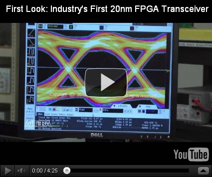
20nm 32-Gbps transceiver from Altera

Altera_20nm_transceiver Altera has announced the successfull demonstration of a programmable device, with 32-Gbps transceiver capabilities, based on TSMC's 20SoC process technology.

The company states that this validates the performance capabilities of 20nm silicon and is a positive indicator for next-generation devices in performance demanding, bandwidth-centric applications.

“Today’s news represents a significant milestone for the industry and for the transceiver development team at Altera,” said Vince Hu, vice president of product and corporate marketing at Altera.

“These 20 nm devices contain the key IP components that will be included in our next-generation FPGAs and validating them now provides us confidence we will deliver to the market 20 nm FPGAs on schedule.”

For more information, see www.altera.com/32gbps-20nm

Get free daily email updates!

Follow us!

Tuesday, 15 January 2013

SEMI Industry spending $32.4B this year on IC gear

ics Fab equipment spending saw a drastic dip in 2H12 and 1Q13 is expected to be even lower, says SEMI, which reckons that the projected number of facilities equipping will drop from 212 in 2012 to 182 in 2013.

Spending on fab equipment for System LSI is expected to drop in 2013. Spending for Flash declined rapidly in 2H12 (by over 40 %) but is expected to pick up by 2H13. The foundry sector is expected to increase spending in 2013, led by major player TSMC, as well as Samsung and Global foundries.

Fab construction:
While fab construction spending slowed in 2012, at -15%,  SEMI  projects an increase of 3.7 % in 2013 (from $5.6bn in 2012 to $5.8bn  in 2013).

The report tracks 34 fab construction projects for 2013 (down from 51 in 2012).  An additional 10 new construction projects with various probabilities may start in 2013. The largest increase for construction spending in 2013 is expected to be for dedicated foundries and Flash related facilities.

Many device manufacturers are hesitating to add capacity due to declining average selling prices and high inventories.

However SEMI reckons flash capacity will grow 6%  by mid-2013, with nearly 6 % growth, adding over 70,000wpm.

SEMI also foresees a rapid increase of installed capacity for new technology nodes, not only for 28nm but also from 24nm to 18nm and first ramps for 17nm to 13nm in 2013.

SEMI cautiously forecasts  fab equipment spending in 2013 to range from minus 5 to plus 3.

Get free daily email updates!

Follow us!

Sunday, 13 January 2013

Full Speed Ahead For FPGA

droppedImageIn the world of high-frequency trading, where speed matters most, technology that can gain a crucial split-second advantage over a rival is valued above all others.

And in what could be the next phase of HFT, firms are looking more and more to hardware solutions, such as field-programmable gate array (FPGA), as it can offer speed gains on the current software used by HFT firms.

FPGA technology, which allows for an integrated circuit to be designed or configured after manufacturing, has been around for decades but has only been on the radar of HFT firms for a couple of years. But new solutions are beginning to pop up that may eventually see FPGA become more viable and be the latest must-have tool in the high-speed arms race.

For instance, a risk calculation that can take 30 microseconds to perform by a software-based algorithm takes just three microseconds with FPGA.

Current HFT platforms are typically implemented using software on computers with high-performance network adapters. However, the downside of FPGA is that it is generally complicated and time consuming to set up, as well as to re-program, as the programmer has to translate an algorithm into the design of an electronic circuit and describe that design in specialized hardware description language.

The programming space on FPGA is also limited, so programs can’t be too big currently. Although, some tasks such as ‘circuit breakers’ are an ideal current use for FPGA technology.

It is the drawbacks, as well as the costs involved, that are, at present, are holding back trading firms from taking up FPGA in greater numbers. However, because of the speed gains that it offers, much resources are being poured into FPGA in a bid to make the technology more accessible—and some technology firms are now beginning to claim significant speed savings with their products.

Cheetah Solutions, a provider of hardware solutions for financial trading, is one firm that says it can now offer reconfigurable FPGA systems to trading firms. It says its Cheetah Framework provides building blocks which can be configured in real time by a host server and an algorithm can execute entirely in an FPGA-enabled network card with the server software taking only a supervisory role by monitoring the algo’s performance and adapting the hardware algo on the go.

“True low latency will only be achieved through total hardware solutions which guarantee deterministic low latency,” said Peter Fall, chief executive of Cheetah Solutions. “But if the market moves, you want to be able to tweak an algorithm or change it completely to take advantage of current conditions. Traditional FPGA programming may take weeks to make even a simple change whereas Cheetah Framework provides on-the-fly reconfigurability.”

Another technology firm to claim that it can make automated trading strategies even faster and more efficient is U.K.-based Celoxica, which recently debuted its new futures trading platform, based on FPGA technology, which involves a circuit on one small chip that can be programmed by the customer.

Celoxica says the platform is designed to accelerate the flow of market data into trading algorithms to make trading faster. It covers multiple trading strategies and asset classes including fixed income, commodities and foreign exchange.

“For futures trading, processing speed, determinism and throughput continue to play a crucial role in the success of principle trading firms and hedge funds trading on the global futures markets,” said Jean Marc Bouleier, chairman and chief executive at Celoxica. “Our clients and partners can increase focus on their trading strategies for CME, ICE, CFE, Liffe US, Liffe and Eurex.”

While last August, Fixnetix, a U.K. trading technology firm, said that it had signed up a handful of top-tier brokers to use its FPGA hardware chip, which executes deals, compliance and risk checks, suggesting that this niche technology is picking up speed rapidly.

Thursday, 6 September 2012

Choosing FPGA or DSP for your Application


FPGA or DSP - The Two Solutions

The DSP is a specialised microprocessor - typically programmed in C, perhaps with assembly code for performance. It is well suited to extremely complex maths-intensive tasks, with conditional processing. It is limited in performance by the clock rate, and the number of useful operations it can do per clock. As an example, a TMS320C6201 has two multipliers and a 200MHz clock – so can achieve 400M multiplies per second.

In contrast, an FPGA is an uncommitted "sea of gates". The device is programmed by connecting the gates together to form multipliers, registers, adders and so forth. Using the Xilinx Core Generator this can be done at a block-diagram level. Many blocks can be very high level – ranging from a single gate to an FIR or FFT. Their performance is limited by the number of gates they have and the clock rate. Recent FPGAs have included Multipliers especially for performing DSP tasks more efficiently. – For example, a 1M-gate Virtex-II™ device has 40 multipliers that can operate at more than 100MHz. In comparison with the DSP this gives 4000M multiplies per second.


Where They Excel


When sample rates grow above a few Mhz, a DSP has to work very hard to transfer the data without any loss. This is because the processor must use shared resources like memory busses, or even the processor core which can be prevented from taking interrupts for some time. An FPGA on the other hand dedicates logic for receiving the data, so can maintain high rates of I/O.

A DSP is optimised for use of external memory, so a large data set can be used in the processing. FPGAs have a limited amount of internal storage so need to operate on smaller data sets. However FPGA modules with external memory can be used to eliminate this restriction.

A DSP is designed to offer simple re-use of the processing units, for example a multiplier used for calculating an FIR can be re-used by another routine that calculates FFTs. This is much more difficult to achieve in an FPGA, but in general there will be more multipliers available in the FPGA. 

If a major context switch is required, the DSP can implement this by branching to a new part of the program. In contrast, an FPGA needs to build dedicated resources for each configuration. If the configurations are small, then several can exist in the FPGA at the same time. Larger configurations mean the FPGA needs to be reconfigured – a process which can take some time.

The DSP can take a standard C program and run it. This C code can have a high level of branching and decision making – for example, the protocol stacks of communications systems. This is difficult to implement within an FPGA.

Most signal processing systems start life as a block diagram of some sort. Actually translating the block diagram to the FPGA may well be simpler than converting it to C code for the DSP.

Making a Choice

There are a number of elements to the design of most signal processing systems, not least the expertise and background of the engineers working on the project. These all have an impact on the best choice of implementation. In addition, consider the resources available – in many cases, I/O modules have FPGAs on board. Using these with a DSP processor may provide an ideal split.


As a rough guideline, try answering these questions:

  1. What is the sampling rate of this part of the system? If it is more than a few MHz, FPGA is the natural choice.
  2. Is your system already coded in C? If so, a DSP may implement it directly. It may not be the highest performance solution, but it will be quick to develop.
  3. What is the data rate of the system? If it is more than perhaps 20-30Mbyte/second, then FPGA will handle it better.
  4. How many conditional operations are there? If there are none, FPGA is perfect. If there are many, a software implementation may be better.
  5. Does your system use floating point? If so, this is a factor in favour of the programmable DSP. None of the Xilinx cores support floating point today, although you can construct your own.
  6. Are libraries available for what you want to do? Both DSP & FPGA offer libraries for basic building blocks like FIRs or FFTs. However, more complex components may not be available, and this could sway your decision to one approach or the other.

In reality, most systems are made up of many blocks. Some of those blocks are best implemented in FPGA, others in DSP. Lower sampling rates and increased complexity suit the DSP approach; higher sampling rates, especially combined with rigid, repetitive tasks, suit the FPGA.


Some Examples

Here are a few examples of signal processing blocks, along with how we would implement them:

  1. First decimation filter in a digital wireless receiver. Typically, this is a CIC filter, operating at a sample rate of 50-100MHz. A 5-stage CIC has 10 registers & 10 adds, giving an "add rate" of 500-1000MHz.
    At these rates any DSP processor would find it extremely difficult to do anything. However, the CIC has an extremely simple structure, and implementing it in an FPGA would be easy. A sample rate of 100MHz should be achievable, and even the smallest FPGA will have a lot of resource left for further processing.
  2. Communications Protocol Stack – ISDN, IEEE1394 etc; these are complex large pieces of C code, completely unsuitable for the FPGA. However the DSP will implement them easily. Not only that, a single code base can be maintained, allowing the code stack to be implemented on a DSP in one product, or a separate control processor in another; and bringing the opportunity to licence the code stack from a specialist supplier.
  3. Digital radio receiver – baseband processing. Some receiver types would require FFTs for signal acquisition, then matched filters once a signal is acquired. Both blocks can be easily implemented by either approach. However, there is a mode change – from signal acquisition to signal reception.
    It may well be that this is better suited to the DSP, as the FPGA would need to implement both blocks simultaneously. Note that the RF processing is better in an FPGA, so this is likely to be a mixed system.
    (Note – with today’s larger FPGAs, both modes of this system could be included in the FPGA at the same time.)
  4. Image processing. Here, most of the operations on an image are simple and very repetitive – best implemented in an FPGA. However, an imaging pipeline is often used to identify "blobs" or "Regions of Interest" in an object being inspected. These blobs can be of varying sizes, and subsequent processing tends to be more complex. The algorithms used are often adaptive, depending on what the blob turns out to be… so a DSP-based approach may be better for the back end of the imaging pipeline.

Summary

FPGA and DSP represent two very different approaches to signal processing – each good at different things. There are many high sampling rate applications that an FPGA does easily, while the DSP could not. Equally, there are many complex software problems that the FPGA cannot address.

Wednesday, 29 August 2012

Altera’s 28-nm Stratix V FPGAs- Contains Industry’s Fastest Backplane-capable Transceivers

San Jose, Calif., July 31, 2012—Altera Corporation (Nasdaq: ALTR) today announced it is shipping in volume production the FPGA industry’s highest performance backplane-capable transceivers. Altera’s Stratix® V FPGAs are the industry’s only FPGAs to offer 14.1 Gbps transceiver bandwidth and are the only FPGAs capable of supporting the latest generation of the Fibre Channel protocol (16GFC). Developers of backplanes, switches, data centers, cloud computing applications, test and measurement systems and storage area networks can achieve significantly higher data rate speeds as well as rapid storage and retrieval of information by leveraging Altera’s latest generation 28-nm high-performance FPGA. For OTN (optical transport network) applications, Stratix V FPGAs allow carriers to scale quickly to support the tremendous growth of traffic on their networks.

Altera started shipping engineering samples of 28-nm FPGAs featuring integrated 14.1 Gbps transceivers over one year ago. These high-performance devices are the latest in Altera’s 28-nm FPGA portfolio to ship in volume production. The transceivers in Stratix V GX and Stratix V GS FPGAs deliver high system bandwidth (up to 66 lanes operating up to 14.1 Gbps) at the lowest power consumption (under 200 mW per channel). Transceivers in Altera’s FPGAs are equipped with advanced equalization circuit blocks, including low-power CTLE (continuous time linear equalization), DFE (decision feedback equalization), and a variety of other signal conditioning features for optimal signal integrity to support backplane, optical module, and chip-to-chip applications. This advanced signal conditioning circuitry enables direct drive of 10GBASE-KR backplanes using Stratix V FPGAs.

“Developers of next-generation protocols need to leverage the latest test equipment that integrates the latest technologies,” said Michael Romm, vice president of product development, at LeCroy Protocol Solutions Group, a leading manufacturer of test and measurement equipment. “Altera’s latest family of 28-nm FPGAs gives us the capability to build the most sophisticated and advanced test equipment so our customers can rapidly develop and bring to market their next-generation systems.”


Published by Altera, click here to read the whole article.