Featured post

Top 5 books to refer for a VHDL beginner

VHDL (VHSIC-HDL, Very High-Speed Integrated Circuit Hardware Description Language) is a hardware description language used in electronic des...

Monday, 4 July 2011

Synchronous Counter

The purpose of writing this is to collate information on Digital Synchronous Counters. Particular emphasis was placed on the following areas :

1. Types of Synchronous Counters and How they work

2. Fast Counter Techniques

3. Implementation of Counters :

4. Dedicated Hardware and Alternative Devices

According to the Oxford Encyclopædic Dictionary:

synchronous adj. existing or occurring at the same time.

counter n. an apparatus used for counting. || a person or thing that counts.

So a "synchronous counter" should mean "a person, thing or apparatus that counts at the same time" ?!?! Hmmm...

Let us take a look at the definition given by the IBM Dictionary of Computing instead.

synchronous (1) Pertaining to two or more processes that depend upon the occurrence of specific events such as common timing signals. (2) Occurring with a regular or predictable time relationship.

counter (1) A functional unit with a finite number of states each of which represents a number that can be, upon receipt of an appropriate signal, increased by unity or by a given constant. This device is usually capable of bringing the represented number to a specified value; for example zero.

So a "synchronous counter" is actually a functional unit with a certain number of states, each representing a number which can be increaced or decreased upon receiving an appropriate signal (e.g. a rising edge pulse), and is usually used to count to, or count down to zero from, a specified number N.

... and what it "really" means. OK! Enough of dictionary definitions.

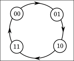
Basically, any sequential circuit that goes through a prescribed sequence of states upon the application of input pulses is called a counter. The input pulses, called count pulses, may be clock pulses or they may originate from an external source and may occur at prescribed intervals of time or at random. The sequence of states in a counter may follow a binary count or any other sequence.

Counter_State_Maching


Read More

Sunday, 3 July 2011

VLSI FPGA Projects Topics Using VHDL/Verilog

    1. 8-bit Micro Processor

    2. RISC Processor in VLDH

    3. Floating Point Unit

    4. LFSR - Random Number Generator

    5. Versatile Counter

    6. RS232 interface

    7. I2C Slave

    8. 8b10b Encoder/Decoder

    9. Floating Point Adder and Multiplier

    10. Progressive Coding For Wavelet-Based Image Compression

    11. An Area-Efficient Universal Cryptography Processor for Smart Cards

    12. FPGA Based Power Efficient Channelizer for Software Defined Radio

    13. Implementation of IEEE 802.11a WLAN baseband Processor using FPGA with Verilog/VHDL code

    14. FPGA Implementation of USB Transceiver Macrocell Interface with Usb2.0 Specifications

    15. Design of a Multi-Mode Receive Digital-Front-End for Cellular Terminal RFIC

    16. Superscalar Power Efficient Fast Fourier Transform FFT Architecture

    17. High-Speed Architecture for Reed-Solomon Decoder/Encoder

    18. Fault Secure Encoder and Decoder for Nano-memory Applications

    19. Implementation Huffman Coding For Bit Stream Compression In Mpeg – 2

    20. Implementation of Hash Algorithm Used for Cryptography And Security

    21. Implementation of Scramblers and Descramblers in Fiber Optic Communication Systems – SONET and OTN

    22. Implementation of Matched Filters Frequency Spectrum in Code Division Multiple Access (CDMA) System and its Implementation

    23. High Definition HDTV Data Encoding and Decoding using Reed Solomon Code

    24. Design & Implementation of Noise / Echo canceler using FPGA with Verilog/VHDL

    25. A VLSI Architecture for Visible Watermarking In A Secure Still Digital Camera (S2dc) Design

    26. FPGA-Based Architecture for Real Time Image Feature Extraction

    27. Implementation of Lossless Data Compression and Decompression using (Parallel Dictionary Lempel Ziv Welch) PDLZW Algorithm

    28. 8/16/32 Point Fast Fourier Transform Algorithm using FPGA with Verilog/VHDL

    29. VLSI Implementation of Booths Algorithm using FPGA with Verilog/VHDL

    30. Design of a Multi-Mode Receive Digital-Front-End for Cellular Terminal RFICs

    31. VLSI implementation of Cascaded-Integrator-Comb Filter

    32. VLSI implementation of Wave-Digital-Filters

    33. VLSI implementation of Notch filters

    34. VLSI implementation of fractional sample rate converter (FSRC) and corresponding converter architecture

    35. VLSI implementation of canonical Huffman encoder/decoder algorithm using FPGA with Verilog/VHDL code

    36. VLSI implementation of RC5 Encryption/Decryption Algorithm

    37. VLSI implementation of Steganography using FPGA with Verilog/VHDL code

    38. VLSI implementation of 16 Bit fixed point DSP Processor using FPGA with Verilog/VHDL

    39. VLSI Implementation of Address Generation Coprocessor

    40. VLSI Implementation of AHDB (Adaptive Huffman Dynamic Block) Algorithm

    41. Implementation of LZW Data Compression Algorithm.

    42. A Low Power VLSI Implementation for JPEG2000 Codec using FPGA with Verilog/VHDL

    43. A Verilog Implementation of Built In Self Test of UART

    44. Fuzzy based PID Controller using VHDL for Transportation Application

    45. VLSI Architecture and FPGA Prototyping of a Digital Camera for Image Security and Authentication

    46. Scalable multi gigabit pattern matching for packet inspection

    47. An FPGA-based Architecture for Real Time Image Feature Extraction

    48. Synchronization in Software Radios – Carrier and Timing Recovery Using FPGAs

    49. Optimized Software Implementation of a Full-Rate IEEE 802.11a Compliant Digital Baseband Transmitter on a Digital Signal Processor

    50. High-Speed Booth Algorithm Encoded Parallel Multiplier Design

    51. Implementation of IEEE 802.11a WLAN Baseband Processor

    52. MPEG-4 AVClH.264 Transform Coding Design using FPGA with Verilog/VHDL

    53. FPGA based Generation of High Frequency Carrier for Pulse Compression using CORDIC Algorithm

    54. Watermarking in a Secure Still Digital Camera Design

    55. DCT/IDCT Algorithms Implemented in FPGA Chips for Real-Time Image Compression

    56. VLSI Architecture and FPGA Prototyping of a Digital Camera for Image Security and Authentication

    57. Robust Image Watermarking Based on Multiband Wavelets and Empirical Mode Decomposition

    58. A VLSI Architecture for Visible Watermarking in a Secure Still Digital Camera (S2DC) Design

    59. VLSI Design & Implementation of Cryptography AES/DES Encryption Algorithm using FPGA with Verilog/VHDL code

    60. VLSI Design & Implementation of Viterbi Algorithm-Encoder/Decoder using FPGA with Verilog/VHDL code

    61. VLSI Design & Implementation of DDRR Algorithm using FPGA with Verilog/VHDL code

    62. VLSI Design & Implementation of Dynamic/Deficit Round Robin Algorithm using FPGA with Verilog/VHDL code

    63. VLSI Design & Implementation of Watermarking Algorithm using FPGA with Verilog/VHDL code

    64. VLSI Design & Implementation of Secure transmitting and receiving text data in communication systems using FPGA with Verilog/VHDL code

    65. VLSI Design & Implementation of UART Asynchronous Transmitter/Receiver using FPGA with Verilog/VHDL code

    66. VLSI Design & Implementation of RS-232 Transmitter/Receiver using FPGA with Verilog/VHDL code

    67. VLSI Design & Implementation of Asynchronous Serial controller using FPGA with Verilog/VHDL code

    68. VLSI Design & Implementation of Universal Serial Bus USB Device Controller using FPGA with Verilog/VHDL code

    69. VLSI Design & Implementation of GPS-GSM based Home Automation System using FPGA with Verilog/VHDL code

    70. VLSI Design & Implementation of 16/32/64-bit Low Power RISC/CISC Processor using FPGA with Verilog/VHDL code

    71. VLSI Design & Implementation of Multichannel I2S Audio Controller using FPGA with Verilog/VHDL code

    72. VLSI Design & Implementation of Asynchronous FIFO using FPGA with Verilog/VHDL code

    73. VLSI Design & Implementation of AHB Master/Slave using FPGA with Verilog/VHDL code

    74. VLSI Design & Implementation of AMBA AHB to PVCI Bridge using FPGA with Verilog/VHDL code

    75. VLSI Design & Implementation of Huffman Encoder/Decoder using FPGA with Verilog/VHDL code

    76. VLSI Design & Implementation of Programmable 16-Tap FIR Filter using FPGA with Verilog/VHDL code

    77. VLSI Design & Implementation of 2-D Convolution Engine using FPGA with Verilog/VHDL code

    78. VLSI Design & Implementation of VGA/LCD Controller using FPGA with Verilog/VHDL code

    79. VLSI Design & Implementation of JTAG TAP controller using FPGA with Verilog/VHDL code

    80. VLSI Design & Implementation of Booth Multiplier using FPGA with Verilog/VHDL code

    81. VLSI Design & Implementation of Pipeline JPEG Encoder using FPGA with Verilog/VHDL code

    82. VLSI Design & Implementation of Cyclic Redundancy Check ECRC/LCRC Error Check using FPGA with Verilog/VHDL code

    83. VLSI Design & Implementation of Vehicle Tracking & Safety System using FPGA with Verilog/VHDL code

    84. VLSI Design & Implementation of Low Power FIR Filter using FPGA with Verilog/VHDL code

    85. VLSI Design & Implementation of Pattern Generator using FPGA with Verilog/VHDL code

    86. VLSI Design & Implementation of PCI Express using FPGA with Verilog/VHDL code

    87. VLSI Design & Implementation of Highspeed USB 2.0/Superspeed USB 3.0 Transmitter and Receiver using FPGA with Verilog/VHDL code

    88. VLSI Design & Implementation of Wishbone Controller using FPGA with Verilog/VHDL code

    89. VLSI Design & Implementation of PVCI Master/Slave using FPGA with Verilog/VHDL code
Get free daily email updates!

Follow us!

Thursday, 30 June 2011

Clock Skew In Sequential Circuits

Differences in clock signal arrival times across the chip are called clock skew. It is a fundamental design principle that timing must satisfy register setup and hold time requirements. Both data propagation delay and clock skew are parts of these calculations. Clocking sequentially-adjacent registers on the same edge of a high-skew clock can potentially cause timing violations or even functional failures.

Below Figure 1 shows an example of sequentially-adjacent registers, where a local routing resource has been used to route the clock signal. In this situation, a noticeable clock skew is likely.

In Figure 1, all registers are clocked at the same edge, but the arrival time of the edge is different at each register. Figure 2 indicates an example of the clock skew for the circuit shown in Figure 1.

Clock_skew_in_registerFigure 1: Sequentially Adjacent Registers with Clock Skew

Clock_skew_timing_diagramFigure 2: Clock Arrival Time Functions in the Circuit of Figure 1

History Of Verilog HDL

Verilog was started initially as a proprietary hardware modeling language by Gateway Design Automation Inc. around 1984. It is rumored that the original language was designed by taking features from the most popular HDL language of the time, called HiLo, as well as from traditional computer languages such as C. At that time, Verilog was not standardized and the language modified itself in almost all the revisions that came out within 1984 to 1990.

Verilog simulator was first used beginning in 1985 and was extended substantially through 1987. The implementation was the Verilog simulator sold by Gateway. The first major extension was Verilog-XL, which added a few features and implemented the infamous "XL algorithm" which was a very efficient method for doing gate-level simulation.

The time was late 1990. Cadence Design System, whose primary product at that time included Thin film process simulator, decided to acquire Gateway Automation System. Along with other Gateway products, Cadence now became the owner of the Verilog language, and continued to market Verilog as both a language and a simulator. At the same time, Synopsys was marketing the top-down design methodology, using Verilog. This was a powerful combination.

In 1990, Cadence recognized that if Verilog remained a closed language, the pressures of standardization would eventually cause the industry to shift to VHDL. Consequently, Cadence organized the Open Verilog International (OVI), and in 1991 gave it the documentation for the Verilog Hardware Description Language. This was the event which "opened" the language.

OVI did a considerable amount of work to improve the Language Reference Manual (LRM), clarifying things and making the language specification as vendor-independent as possible.

Soon it was realized that if there were too many companies in the market for Verilog, potentially everybody would like to do what Gateway had done so far - changing the language for their own benefit. This would defeat the main purpose of releasing the language to public domain. As a result in 1994, the IEEE 1364 working group was formed to turn the OVI LRM into an IEEE standard. This effort was concluded with a successful ballot in 1995, and Verilog became an IEEE standard in December 1995.

When Cadence gave OVI the LRM, several companies began working on Verilog simulators. In 1992, the first of these were announced, and by 1993 there were several Verilog simulators available from companies other than Cadence. The most successful of these was VCS, the Verilog Compiled Simulator, from Chronologic Simulation. This was a true compiler as opposed to an interpreter, which is what Verilog-XL was. As a result, compile time was substantial, but simulation execution speed was much faster.

In the meantime, the popularity of Verilog and PLI was rising exponentially. Verilog as a HDL found more admirers than well-formed and federally funded VHDL. It was only a matter of time before people in OVI realized the need of a more universally accepted standard. Accordingly, the board of directors of OVI requested IEEE to form a working committee for establishing Verilog as an IEEE standard. The working committee 1364 was formed in mid 1993 and on October 14, 1993, it had its first meeting.

The standard, which combined both the Verilog language syntax and the PLI in a single volume, was passed in May 1995 and now known as IEEE Std. 1364-1995.

After many years, new features have been added to Verilog, and the new version is called Verilog 2001. This version seems to have fixed a lot of problems that Verilog 1995 had. This version is called 1364-2001.

Timeline:

1984 Verilog-XL simulator and language developed by Gateway Design Automation
1987 Synopsys introduced a Verilog based synthesis tool.
1989 Cadence Design Systems acquired Gateway, and Verilog.
1990 Cadence placed the Verilog language in the public domain.
1995 Verilog HDL became (IEEE Std 1364-1995).
1997 Verilog VCS bought by Viewlogic
1997 Viewlogic bought by Synopsys
1998 Synopsys issues Verilog VCS
2001 A significantly revised version was published in 2001.

Wednesday, 29 June 2011

Scriptum - Free VHDL and Verilog Text Editor

Scriptum is a free text editor focused at VHDL and Verilog design, running on Windows and Linux. Using a multiple document window interface combined with tab pages it offers you an slick environment to edit VHDL, Verilog and other language files.

Even on extremely large files Scriptum offers exceptionally fast editing capabilities. You can avoid typing errors and dramatically improve your productivity by using keyword and header templates, identifier repeat, auto case conversion and one-touch line and column manipulation. To keep your text highly readable and well structured, you may choose syntax coloring and in- and out-commenting of selected text, as well as line numbering and indentation. Scriptum offers extensive documentation capabilities such as color coding, capitalization and indentation to make your numerous lines of code more readable. Scriptum is fully customizable to create a design environment that meets your needs. Design language, synthesis templates, keyword templates, and user interface are easily tailored to your requirements.

Features

  • Syntax color highlighting
  • Code folding for VHDL & Verilog
  • Manual Code folding
  • Code templates
  • Block and Column selections
  • Selection Indenting / De-indenting
  • Selection Commenting / Uncommenting
  • Tabs and spaces conversion
  • White space viewer

Language support

Scriptum comes standard with support for the following languages:
  • Verilog
  • VHDL
  • Tcl
  • SystemC
  • Perl
  • Java
  • Edif
  • C/C++
  • Actel PDC
  • Altera QSF
  • Xilinx UCF
Additional languages can be added using Scriptum configuration files.

Download Scriptum 10 now (FREE):

DOWNLOAD

Wednesday, 22 June 2011

4x1 Multiplexer Using 2x1 Multiplexer

Below Fig. shows the way to build 4x1 Multiplexer using three 2x1 Multiplexers.

4x1_mux_using_2x1_mux

Get free daily email updates!

Follow us!

Wednesday, 15 June 2011

Seven steps to a bootable Windows 7 thumb drive

Yesterday i thought to install windows 7 to my pc using a bootable windows 7 thumb drive, but creating a bootable USB drive for windows 7 is very complicated.

There are plenty of great tutorials out there that basically contain the same information as this one, but I thought I’d try to put together a how-to guide that made everything as simple as possible for people who might like the idea of Windows on a thumb drive but aren’t necessarily super comfortable with the actual process.
The only tangible thing you’ll need is a USB thumb drive with at least 4GB of capacity. I found a SanDisk Cruzer Contour worked best, while a Kingston DataTraveler was a bit fidgety at first but worked after a couple of tries.
It’s all pretty easy once you get going, so let’s begin.
Step One: Download Windows 7 Beta

Head over to http://www.microsoft.com/windows/windows-7/beta-download.aspxand jump through all the hoops to begin your download. For the sake of this exercise, we’ll assume that you’ll download the ISO file to your desktop. The download might take a while depending on your connection speed – set aside an hour to be on the safe side. Meanwhile, take a break. You’ve earned it!
Step Two: Download and install WinRAR

I hate guides that make me go download a bunch of software just to accomplish a task, so I apologize for making you do the same thing. I promise this will be the only third-party software that you’ll have to download and install, though, and it’s a great program to have on your computer anyway if you don’t already.
Head over to http://rarsoft.com/download.htm and click on the WinRAR 3.80 link to download the software. Once downloaded, install it.
Step Three: Extract the Windows 7 ISO file

Once Windows 7 Beta has finished downloading, you should see a file on your desktop with a bunch of gobbledygook in the name like “7000.0.081212-1400_client_en-us_Ultimate-GB1CULFRE_EN_DVD” or something cryptic like that. Right-click on that file and choose “Extract to [gobbledygook]” as shown in the above picture. When the smoke has cleared, you’ll have a gobbledygook folder on your desktop. I’ll continue to refer to this folder as “the gobbledygook folder” for the rest of this guide.
Step Four: Format a 4GB USB thumb drive

Head into “Computer” or “My Computer” and locate your USB thumb drive. In this instance, we’re dealing with the F: drive. Right click on the drive and choose “Format…” Then, we want to format the drive using the NTFS file system with the default allocation size, so make sure those two things are selected from the dropdown menus. You can check the Quick Format box, too, if it’s not already checked.
Step Five: The tricky BootSect.exe part

Now we’re going to go back to our extracted “7000.0.081212-1400_client_en-us_Ultimate-GB1CULFRE_EN_DVD” gobbledygook folder and open the “boot” folder, inside which we’ll find a file called “bootsect.exe” that we’ll need to use.
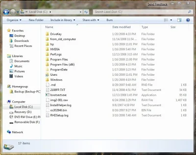
If you’re comfortable navigating folders in DOS, then you can skip this particular step. If you don’t like DOS or haven’t used it much, we’re going to copy this bootsect.exe file into an easy-to-access location. Copy the file (CTRL-C) and then open up “Computer” or “My Computer” and double-click your C: drive.

We’re going to paste (CTRL-V) that “bootsect.exe” file right into C: so we can easily access it in a moment. See it there? Fifth file from the bottom, all safe and sound?
Step Six: Do some Ninja-like stuff in DOS

Now we’re going to open the Command Prompt. If you’re using Vista or Windows 7, you’ll have to do the “Run as administrator” thing or we won’t be able to deploy our sweet flanking maneuvers that are coming up. So go into Programs > Accessories and then right-click on Command Prompt and choose “Run as administrator.”

Once we’ve got the Command Prompt up, we’re going to switch to our top-level C: folder by simply typing “cd\” without the quotes and hitting Enter (If you skipped Step Five above, then navigate yourself to the “boot” folder inside the extracted ISO folder on your desktop).

We should then have a straight-up C:> prompt. At this point, we’ll type the following (without the quotes):
“bootsect /nt60 f:”
We’re assuming the drive letter of your USB thumb drive is F:, so replace “f:” in the above phrase with whichever letter is assigned to your particular thumb drive. Hit enter and you should see:

Blah, blah, blah your bootcode is something something. This just means that the thumb drive is now ripe to auto-load when you boot up your computer.
Step Seven: Copy the Windows 7 files to the thumb drive

This is it! The final step! Open up your extracted Windows 7 gobbledygook folder and copy the files over to your thumb drive. You should be copying five folders and three files to the thumb drive. That is, don’t drag the gobbledygook folder over; open it up first and drag the stuff inside of it over instead.

It’ll take maybe about ten minutes for everything to copy over. Take another break! You’ve earned it!
When all is said and done, reboot your computer with the thumb drive in place and you should be greeted with the Windows 7 installation menu. If you’re not, you might have to tweak your BIOS settings to allow your computer to recognize a thumb drive as a bootable device.