Featured post

Top 5 books to refer for a VHDL beginner

VHDL (VHSIC-HDL, Very High-Speed Integrated Circuit Hardware Description Language) is a hardware description language used in electronic des...

Wednesday, 29 August 2012

Altera’s 28-nm Stratix V FPGAs- Contains Industry’s Fastest Backplane-capable Transceivers

San Jose, Calif., July 31, 2012—Altera Corporation (Nasdaq: ALTR) today announced it is shipping in volume production the FPGA industry’s highest performance backplane-capable transceivers. Altera’s Stratix® V FPGAs are the industry’s only FPGAs to offer 14.1 Gbps transceiver bandwidth and are the only FPGAs capable of supporting the latest generation of the Fibre Channel protocol (16GFC). Developers of backplanes, switches, data centers, cloud computing applications, test and measurement systems and storage area networks can achieve significantly higher data rate speeds as well as rapid storage and retrieval of information by leveraging Altera’s latest generation 28-nm high-performance FPGA. For OTN (optical transport network) applications, Stratix V FPGAs allow carriers to scale quickly to support the tremendous growth of traffic on their networks.

Altera started shipping engineering samples of 28-nm FPGAs featuring integrated 14.1 Gbps transceivers over one year ago. These high-performance devices are the latest in Altera’s 28-nm FPGA portfolio to ship in volume production. The transceivers in Stratix V GX and Stratix V GS FPGAs deliver high system bandwidth (up to 66 lanes operating up to 14.1 Gbps) at the lowest power consumption (under 200 mW per channel). Transceivers in Altera’s FPGAs are equipped with advanced equalization circuit blocks, including low-power CTLE (continuous time linear equalization), DFE (decision feedback equalization), and a variety of other signal conditioning features for optimal signal integrity to support backplane, optical module, and chip-to-chip applications. This advanced signal conditioning circuitry enables direct drive of 10GBASE-KR backplanes using Stratix V FPGAs.

“Developers of next-generation protocols need to leverage the latest test equipment that integrates the latest technologies,” said Michael Romm, vice president of product development, at LeCroy Protocol Solutions Group, a leading manufacturer of test and measurement equipment. “Altera’s latest family of 28-nm FPGAs gives us the capability to build the most sophisticated and advanced test equipment so our customers can rapidly develop and bring to market their next-generation systems.”


Published by Altera, click here to read the whole article.

Sunday, 26 August 2012

Inside TSMC – A FAB Tour

An up to date and current overview of semiconductor manufacturing technology from TSMC in Taiwan. Nicely produced and informative if you tune-out the voice-over slightly. Better access than any Fab tour.
Recommended if you have any interest in how semiconductors are made/manufactured in volume right now.

In the microelectronics industry a semiconductor fabrication plant (commonly called a fab) is a factory where devices such as integrated circuits are manufactured.

A business that operates a semiconductor fab for the purpose of fabricating the designs of other companies, such as fabless semiconductor companies, is known as a foundry. If a foundry does not also produce its own designs, it is known as a pure-play semiconductor foundry.

Fabs require many expensive devices to function. Estimates put the cost of building a new fab over one billion U.S. dollars with values as high as $3–4 billion not being uncommon. TSMC will be investing 9.3 billion dollars in its Fab15 300 mm wafer manufacturing facility in Taiwan to be operational in 2012.

The central part of a fab is the clean room, an area where the environment is controlled to eliminate all dust, since even a single speck can ruin a microcircuit, which has features much smaller than dust. The clean room must also be dampened against vibration and kept within narrow bands of temperature and humidity. Controlling temperature and humidity is critical for minimizing static electricity.

The clean room contains the steppers for photolithography, etching, cleaning, doping and dicing machines. All these devices are extremely precise and thus extremely expensive. Prices for most common pieces of equipment for the processing of 300 mm wafers range from $700,000 to upwards of $4,000,000 each with a few pieces of equipment reaching as high as $50,000,000 each (e.g. steppers). A typical fab will have several hundred equipment items.

Taiwan Semiconductor Manufacturing Company, Limited or TSMC is the world's largest dedicated independent semiconductor foundry, with its headquarters and main operations located in the Hsinchu Science Park in Hsinchu, Taiwan.

Facilities at TSMC:

  1. One 150 mm (6 inches) wafer fab in full operation (Fab 2)
  2. Four 200 mm (8 inches) wafer fabs in full operation (Fabs 3, 5, 6, 8)
  3. Two 300 mm (12 inches) wafer fabs in production (Fabs 12, 14)
  4. TSMC (Shanghai)
  5. WaferTech, TSMC's wholly owned subsidiary 200 mm (8 inches) fab in Camas, Washington, USA
  6. SSMC (Systems on Silicon Manufacturing Co.), a joint venture with NXP Semiconductors in Singapore which has also brought increased capacity since the end of 2002

TSMC announced plans to invest US$9.4 billion to build its third 12-inch (300 mm) wafer fabrication facility in Central Taiwan Science Park (Fab 15), which will use advanced 40 and 20-nanometer technologies. It is expected to become operational by March 2012. The facility will output over 100,000 wafers a month and generate $5 billion per year of revenue. On January 12, 2011, TSMC announced the acquisition of land from Powerchip Semiconductor for NT$2.9 billion (US$96 million) to build two additional 300 mm fabs to cope with increasing global demand. Further, TSMC has disclosed plans that it will build a 450-mm fab, which may begin its pilot lines 2013, and production as early as 2015.

Tuesday, 21 August 2012

Blocking and Non-Blocking Assignment

keysymbols: =, <=.

Blocking (the = operator)

With blocking assignments each statement in the same time frame is executed in sequential order within their blocks. If there is a time delay in one line then the next statement will not be executed until this delay is over.

integer a,b,c,d;

initial begin
a = 4; b = 3; example 1
#10 c = 18;
#5 d = 7;
end

Above, at time=0 both a and b will have 4 and 3 assigned to them respectively and at time=10, c will equal 18 and at time=15, d will equal 7.

Non-Blocking (the <= operator)


Non-Blocking assignments tackle the procedure of assigning values to variables in a totally different way. Instead of executing each statement as they are found, the right-hand side variables of all non-blocking statements are read and stored in temporary memory locations. When they have all been read, the left-hand side variables will be determined. They are non-blocking because they allow the execution of other events to occur in the block even if there are time delays set.

integer a,b,c;

initial begin
a = 67;
#10;
a <= 4; example 2
c <= #15 a;
d <= #10 9;
b <= 3;
end

This example sets a=67 then waits for a count of 10. Then the right-hand variables are read and stored in tempory memory locations. Here this is a=67. Then the left-hand variables are set. At time=10 a and b will be set to 4 and 3. Then at time=20 d=9. Finally at time=25, c=a which was 67, therefore c=67.

Note that d is set before c. This is because the four statements for setting a-d are performed at the same time. Variable d is not waiting for variable c to complete its task. This is similar to a Parallel Block.

This example has used both blocking and non-blocking statements. The blocking statement could be non-blocking, but this method saves on simulator memory and will not have as large a performance drain.

Application of Non-Blocking Assignments:

We have already seen that non-blocking assignments can be used to enable variables to be set anywhere in time without worrying what the previous statements are going to do.

Another important use of the non-blocking assignment is to prevent race conditions. If the programmer wishes two variables to swap their values and blocking operators are used, the output is not what is expected:

initial begin
x = 5;
y = 3;
end
example 3
always @(negedge clock) begin
x = y;
y = x;
end

This will give both x and y the same value. If the circuit was to be built a race condition has been entered which is unstable. The compliler will give a stable output, however this is not the output expected. The simulator assigns x the value of 3 and then y is then assigned x. As x is now 3, y will not change its value. If the non-blocking operator is used instead:

always @(negedge) begin
x <= y; example 4
y <= x;
end

both the values of x and y are stored first. Then x is assigned the old value of y (3) and y is then assigned the old value of x (5).

Another example when the non-blocking operator has to be used is when a variable is being set to a new value which involves its old value.

i <= i+1;
or examples 5,6
register[5:0] <= {register[4:0] , new_bit};

Race condition in Verilog

In Verilog certain type of assignments or expression are scheduled for execution at the same time and order of their execution is not guaranteed. This means they could be executed in any order and the order could be change from time to time. This non-determinism is called the race condition in Verilog.

Verilog execution order:

verilog_execution

If you look at the active event queue, it has multiple types of statements and commands with equal priority, which means they all are scheduled to be executed together in any random order, which leads to many of the faces..

Lets look at some of the common race conditions that one may encounter.

1) Read-Write or Write-Read race condition.

Take the following example :

always @(posedge clk)
x = 2;

always @(posedge clk)
y = x;

Both assignments have same sensitivity ( posedge clk ), which means when clock rises, both will be scheduled to get executed at the same time. Either first ‘x’ could be assigned value ’2′ and then ‘y’ could be assigned ‘x’, in which case ‘y’ would end up with value ’2′. Or it could be other way around, ‘y’ could be assigned value of ‘x’ first, which could be something other than ’2′ and then ‘x’ is assigned value of ’2′. So depending on the order final value of ‘y’ could be different.

How can you avoid this race ? It depends on what your intention is. If you wanted to have a specific order, put both of the statements in that order within a ‘begin’…’end’ block inside a single ‘always’ block. Let’s say you wanted ‘x’ value to be updated first and then ‘y’ you can do following. Remember blocking assignments within a ‘begin’ .. ‘end’ block are executed in the order they appear.

always @(posedge clk)
begin
x = 2;
y = x;
end

2) Write-Write race condition.

always @(posedge clk)
x = 2;

always @(posedge clk)
x = 9;

Here again both blocking assignments have same sensitivity, which means they both get scheduled to be executed at the same time in ‘active event’ queue, in any order. Depending on the order you could get final value of ‘x’ to be either ’2′ or ’9′. If you wanted a specific order, you can follow the example in previous race condition.

3) Race condition arising from a ‘fork’…’join’ block.

always @(posedge clk)
fork
x = 2;
y = x;
join

Unlike ‘begin’…’end’ block where expressions are executed in the order they appear, expression within ‘fork’…’join’ block are executed in parallel. This parallelism can be the source of the race condition as shown in above example.

Both blocking assignments are scheduled to execute in parallel and depending upon the order of their execution eventual value of ‘y’ could be either ’2′ or the previous value of ‘x’, but it can not be determined beforehand.

4) Race condition because of variable initialization.

reg clk = 0

initial
clk = 1

In Verilog ‘reg’ type variable can be initialized within the declaration itself. This initialization is executed at time step zero, just like initial block and if you happen to have an initial block that does the assignment to the ‘reg’ variable, you have a race condition.

There are few other situations where race conditions could come up, for example if a function is invoked from more than one active blocks at the same time, the execution order could become non-deterministic.

Sunday, 19 August 2012

Asynchronous Integrated Circuits Design

Many modern integrated circuits are sequenced based on globally distributed periodic timing signals called clocks. This method of sequencing, synchronous, is prevalent and has contributed to the remarkable advancements in the semiconductor industry in form of chip density and speed in the last decades. For the trend to continue as proposed in Moore’s law, the number of transistors on a chip doubles about every two years, there are increasing requirements for enormous circuit complexity and transistor down scaling.

As the industry pursues these factors, many problems associated with switching delay, complexity management and clock distribution have placed limitation on the performance of synchronous system with an acceptable level of reliability. Consequently, the synchronous system design is challenged on foreseeable progress in device technology.

These concerns and other factors have caused resurgence in interest in the design of asynchronous or self-timed circuits that achieve sequencing without global clocks. Instead, synchronization among circuit elements is achieved through local handshakes based on generation and detection of request and acknowledgement signals.

Some notable advantages of asynchronous circuits over their synchronous counterparts are presented below:

* Average case performance. Synchronous circuits have to wait until all possible computations have completed before producing the results, thereby yielding the worst-case performance. In the asynchronous circuits, the system senses when computation has completed thereby enabling average case performance. For circuits like ripple carry adders with significantly worst-case delay than average-case delay, this can be an enormous saving in time.

* Design flexibility and cost reduction, with higher level logic design separated from lower timing design

* Separation of timing from functional correctness in certain types of asynchronous design styles thereby enabling insensitivity to delay variance in layout design, fabrication process, and operating environments.

* The asynchronous circuits consume less power than synchronous since signal transitions occur only in areas involved in current computation.

* The problem of clock skew evident in synchronous circuit is eliminated in the asynchronous circuit since there is no global clock to distribute. The clock skew, difference in arrival times of clock signal at different parts of the circuit, is one of the major problems in the synchronous design as feature size of transistors continues to decrease.

Asynchronous circuit design is not entirely new in theory and practice. It has been studied since the early 1940′s when the focus was mainly on mechanical relays and vacuum tube technologies. These studies resulted to two major theoretical models (Huffman and Muller models) in the 1950′s. Since then, the field of asynchronous circuits went through a number of high interest cycles with a huge amount of work accumulated. However, problems of switching hazards and ordering of operations encountered in early complex asynchronous circuits resulted to its replacement by synchronous circuits. Since then, the synchronous design has emerged as the prevalent design style with nearly all the third (and subsequent) generation computers based on synchronous system timing.

Despite the present unpopularity of the asynchronous circuits in the mainstream commercial chip production and some problems noted above, asynchronous design is an important research area. It promises at least with the combination of synchronous circuits to drive the next generation chip architecture that would achieve highly dependable, ultrahigh-performance computing in the 21st century.

The design of the asynchronous circuit follows the established hardware design flow, which involves in order: system specification, system design, circuit design, layout, verification, fabrication and testing though with major differences in concept. A notable one is the impractical nature of designing an asynchronous system based on ad-hoc fashion. With the use of clocks as in synchronous systems, lesser emphasis is placed on the dynamic state of the circuit whereas the asynchronous designer has to worry over hazard and ordering of operations. This makes it impossible to use the same design techniques applied in synchronous design to asynchronous design.

The design of asynchronous circuit begins with some assumption about gate and wire delay. It is very important that the chip designer examines and validates the assumption for the device technology, the fabrication process, and the operating environment that may impact on the system’s delay distribution throughout its lifetime. Based on this delay assumption, many theoretical models of asynchronous circuits have been identified.

There is the delay-insensitive model in which the correct operation of a circuit is independent of the delays in gates and in the wires connecting the gate, assuming that the delays are finite and positive. The speed-independent model developed by D.E. Muller assumes that gate delays are finite but unbounded, while there is no delay in wires. Another is the Huffman model, which assumes that the gate and wire delays are bounded and the upper bound is known.

For many practical circuit designs, these models are limited. For the examples in this discussion, quasi delay insensitive (QDI), which is a combination of the delay insensitive assumption and isochronic-fork assumption, is used. The latter is an assumption that the relative delay between two wires is less than the delay through a sequence of gates. It assumes that gates have arbitrary delay, and only makes relative timing assumptions on the propagation delay of some signals that fan-out to multiple gates.

Over the years, researchers have developed a method for the synthesis of asynchronous circuits whose correct functioning do not depend on the delays of gates and which permitted multiple concurrent switching signals. The VLSI computations are modeled using Communicating Hardware Processes (CHP) programs that describe their behavior algorithmically. The QDI circuits are synthesized from these programs using semantics-preserving transformations.

In conclusion, as the trend continues to build highly dependable, ultrahigh-performance computing in the 21st century, the asynchronous design promises to play a dominant role.

Thursday, 16 August 2012

Refreshing DDR SDRAM

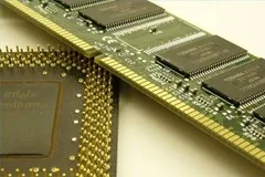
dual-channel-ddr-sdram-800x800 Internally, computer memory is arranged as a matrix of "memory cells" in rows and columns, like the squares on a checkerboard, with each column being further divided by the I/O width of the memory chip. The entire organization of rows and columns is called a DRAM "array." For example, a 2Mx8 DRAM has roughly 2000 rows , 1000 columns, and 8 bits per column -- a total capacity of 16Mb, or 16 million bits.
Each memory cell is used to store a bit of data - stored as an electrical charge - which can be instantaneously retrieved by indicating the data's row and column location; however, DRAM is a volatile form of memory, which means that it must have power in order to retain data. When the power is turned off, data in RAM is lost.
DRAM is called "dynamic" RAM because it must be refreshed, or re-energized, hundreds of times each second in order to retain data. It has to be refreshed because its memory cells are designed around tiny capacitors that store electrical charges. These capacitors work like very tiny batteries and will gradually lose their stored charges if they are not re-energized. Also, the process of retrieving, or reading, data from the memory array tends to drain these charges, so the memory cells must be precharged before reading the data.
Refresh is the process of recharging, or re-energizing, the cells in a memory chip. Cells are refreshed one row at a time (usually one row per refresh cycle). The term "refresh rate" refers, not to the time it takes to refresh the memory, but to the total number of rows that it takes to refresh the entire DRAM array -- e.g. 2000 (2K) or 4000 (4K) rows. The term "refresh cycle" refers to the time it takes to refresh one row or, alternatively, to the time it takes to refresh the entire DRAM array. Refresh can be accomplished in many different ways, which is one of the reasons it can be a confusing topic.
Why are there different types of refresh? How are they different?
Refresh rate is determined by the total number of rows that have to be refreshed in a memory chip. Memory chips are designed for a particular type of refresh. For example, chips using 4K refresh will have about 4000 rows, which means that it will take about 4000 cycles to refresh the entire array. Chips using 2K refresh will have about 2000 rows, and chips with 1K refresh will have about 1000 rows. All of the chips in the chart below have the same total capacity* (16Mb, or 16 million cells), but different numbers of rows and columns depending on the type of refresh used.
4K refresh 2K refresh 1K refresh
4Mx4 4000 rows / 1000 columns 2000 rows / 2000 columns
2Mx8 4000 rows / 500 columns 2000 rows / 1000 columns
1Mx16 4000 rows / 250 columns 1000 rows / 1000 columns
* Capacity = rows x columns x width. For example, a 4Mx4 chip is 4 Megabits "deep" and 4 bits "wide" (Total = 16Mb). If this chip uses 4K refresh, it will be organized into 4000 rows x 1000 columns x 4 bits per column (Total = 16Mb). If this chip uses 2K refresh, it will be internally organized into 2000 rows x 2000 columns x 4 bits per column (Total = 16Mb). The capacity is the same, but the organization and refresh are different.
The major refresh rates in use today are 1K, 2K, 4K, and 8K. The primary reason for these different types of refresh is decreased power consumption. Since column address circuitry requires more power than row address circuitry, using a type of refresh that selects fewer columns per row draws less current -- e.g. 4K versus 2K.
In addition to various refresh rates, there are several different refresh methods. The two most basic methods are distributed and burst. Distributed refresh charges one row at a time, in sequential order. Burst refresh charges a whole group of rows in one burst.
Normally, the refresh operation is initiated by the system's memory controller, but some chips are designed for "self refresh." This means that the DRAM chip has its own refresh circuitry and does not require intervention from the CPU or external refresh circuitry. Self refresh dramatically reduces power consumption and is often used in portable computers.
Two other refresh techniques are hidden and extended refresh. Both of these techniques rely on capacitors (memory cells) that discharge more slowly. Hidden refresh combines the refresh operation with read/write operations. Extended refresh extends the length of time it takes to refresh the entire memory array. The advantage of both is that they do not have to refresh as often.
Why does 4K refresh consume less power than 2K refresh?
It seems logical to think that 4K refresh would consume more power than 2K refresh because the number is larger, but that is not the case. The numbers do not refer to the size of the refresh area but to the number of rows that it takes to refresh the entire DRAM. 2K refresh charges about 2000 rows to refresh a DRAM chip; 4K refresh charges twice as many rows. The tradeoff is that while 4K refresh takes longer, it consumes less power.
In actuality, 4K refresh charges a smaller section of the total array per cycle than 2K refresh. Looking at the chart above, you can see a 4Mx4 chip with 4K refresh charges about 1000 columns for every row, but the same chip with 2K refresh charges about 2000 columns for every row. Remember that column address circuitry requires more power than row address circuitry, so a refresh that charges fewer columns per row draws less current. 4K refresh charges fewer columns per row than 2K refresh and therefore uses less power -- about 1.2x less power.
Is the performance any different for one type of refresh versus another?
Performance differences are miniscule, but a 2K version of one DRAM chip will perform slightly better than a 4K version. The tradeoff between the number of rows and columns in the internal organization affects what is known as the "page depth" of the DRAM chip, which can impact particular applications. On the other hand, a 4K chip consumes much less power. Deciding which type of refresh to use depends on the specific system and application. These specifications are usually detailed by the system manufacturers.
Where are the different types of refresh used?
Most memory chips today use 1K or 2K refresh and can be found in the majority of PCs. At first, 4K refresh was used in portables, workstations, and PC servers because it consumes less power and generates less heat, but 4K refresh is also increasing in desktop PCs. 8K refresh is fairly new and is exclusive to 64Mb chips at present (mostly high-end applications).
Is memory with different refresh rates interchangeable?
The memory controller in your system determines the type of refresh it can support. Some controllers have only enough drivers to support 2K refresh (2000 rows). Others have been designed to support both types of refresh (2K and 4K) using a technique called "redundant addressing." Some support only 4K refresh. It all depends on the system itself.

Friday, 3 August 2012

SystemVerilog Interview Questions

1. What is clocking block?
2. What are modports?
3. What are interfaces?
4. What are virtual interfaces? How can it be used?
5. What is a class?
6. What is program block?
7. What is a mailbox?
8. What are semaphores?
9. Why is reactive scheduler used?
10. What are rand and randc?
11. What is the difference between keywords: rand and randc?
12. What is the use of always_ff?
13. What are static and automatic functions?
14. What is the procedure to assign elements in an array in systemverilog?
15. What are the types of arrays in systemverilog?
16. What are assertions?
17. What is the syntax for ## delay in assertion sequences?
18. What are virtual classes?
19. Why are assertions used?
20. Explain the difference between data type?s logic and reg and wire.
21. What is callback?
22. What are the ways to avoid race condition between testbench and RTL using SystemVerilog?
23. Explain event regions in systemverilog?
24. What are the types of coverages available in systemverilog?
25. How can you detect a deadlock condition in FSM?
26. What is mutex?
27. What is the significance of seed in randomization?
28. What is the difference between code coverage and functional coverage?
29. If the functional coverage is more that code coverage, what does it means?
30. How we can have #delay which is independent of time scale in system verilog?
31. What are constraints in systemverilog?
32. What are the different types of constraints in systemverilog?
33. What is an if-else constraint?
34. What is inheritance and give the basic syntax for it?
35. What is the difference between program block and module?
36. What is final block?
37. What are dynamic and associative arrays?
38. What is an abstract class?
39. What is the difference between $random and $urandom?
40. What is the use of $cast?
41. What is the difference between mailbox and queue?
42. What are bidirectional constraints?
43. What is circular dependency and how to avoid this problem?
44. What is the significance of super keyword?
45. What is the significance of this keyword?
46. What are input and output skews in clocking block?
47. What is a scoreboard?
48. Mention the purpose of dividing time slots in systemverilog?
49. What is static variable?
50. In simulation environment under what condition the simulation should end?
51. What is public declaration?
52. What is the use of local?
53. Difference b/w logic & bit.
54. How to take an asynchronous signal from clocking block?
55. What is fork-join, types and differences?
56. Difference between final and initial blocks?
57. What are the different layers in Testbench?
58. What is the use of modports?
59. What is the use of package?
60. What is the difference between bit [7:0] and byte?
61. What is chandle in systemverilog ?
62. What are the features added in systemverilog for function and task?
63. What is DPI in systemverilog?
64. What is inheritance?
65. What is polymorphism?
66. What is Encapsulation?
67. How to count number of elements in mailbox?
68. What is covergroup?
69. What are super, abstract and concrete classes?
70. Explain some coding guidelines you followed in your environment ?
71. What is Verification plan? What it contains?
72. Explain how messages are handled?
73. What is difference between define and parameter?
74. Why ?always? block not allowed inside program block?
75. How too implement clock in program block?
76. How to kill process in fork/join ?
77. Difference between Associative and dynamic arrays?
78. How to check whether randomization is successful or not?
79. What is property in SVA?
80. What advantages of Assertions?
81. What are immediate Assertions?
82. What are Assertion severity system level task? What happens if we won?t specify these tasks?
83. What is difference between Concurrent and Immediate assertions?
84. In which event region concurrent assertions will be evaluated?
85. What are the main components in Concurrent Assertions?
86. What is Consecutive Repetition Operator in SVA?
87. What is goto Replication operator in SVA?
88. What is difference between x [->4:7] and x [=4:7] in SVA?
89. What are implication operators in Assertions?
90. Can a constructor qualified as protected or local in systemverilog?
91. What are advantages of Interfaces?
92. How automatic variables are useful in Threads?

Get free daily email updates!
Follow us!