Featured post

Top 5 books to refer for a VHDL beginner

VHDL (VHSIC-HDL, Very High-Speed Integrated Circuit Hardware Description Language) is a hardware description language used in electronic des...

Showing posts with label Electronics. Show all posts

Tuesday, 7 October 2014

Transient Materials - Electronics that melt away

transient_materialsImagine tossing your old phone in the toilet, watching it dissolve and then flushing it down, instead of having it wind up in a landfill. Scientists are working on electronic devices that can be triggered to disappear when they are no longer needed.

The technology is years away, but Assistant Professor Reza Montazami and his research team in the mechanical engineering labs at Iowa State University have published a report that shows progress is being made. In the two years they've been working on the project, they have created a fully dissolvable and working antenna.

"You can actually send a signal to your passport via satellite that causes the passport to physically degrade, so no one can use it," Montazami said.

The electronics, made with special "transient materials," could have far-ranging possibilities. Dissolvable electronics could be used in medicine for localizing treatment and delivering vaccines inside the body. They also could eliminate extra surgeries to remove temporarily implanted devices.The military could design information-gathering gadgets that could complete their mission and dissolve without leaving a trace.

The researchers have developed and tested transient resistors and capacitors. They’re working on transient LED and transistor technology, said Montazami, who started the research as a way to connect his background in solid-state physics and materials science with applied work in mechanical engineering.

As the technology develops, Montazami sees more and more potential for the commercial application of transient materials.

Thursday, 23 January 2014

3D graphene-like material promises super electronics

novel-3D-graphene-1Graphane, the thinnest and strongest known material in the universe and a formidable conductor of electricity and heat – gets many of its amazing properties from the fact that it occupies only two dimensions: It has length and width but no height, because it's made of a single layer of atoms. But this special characteristics sometimes makes it difficult to work with, and a challenge to manufacture.

Researchers around the world have looked for ways to take full advantage of its many desirable properties. Now scientists have discovered a material that has a similar electronic structure to graphene but can exist in three dimensions, instead of a flat sheet like graphene, could lead to faster transistors and more compact hard drives.

 Plot of energy levels of electrons in trisodium bismuthide showing that this bulk material has properties similar to graphene.

The material is called three-dimensional topological Dirac semi-metal (3DTDS) and is a form of the chemical compound sodium bismuthate, Na3Bi.

Researchers led by scientists from Oxford University, Diamond Light Source, Rutherford Appleton Laboratory, Stanford University, and Berkeley Lab's Advanced Light Source, has discovered 3DTDS.

'The 3DTDS we have found has a lot in common with graphene and is likely to be as good or even better in terms of electron mobility – a measure of both how fast and how efficiently an electron can move through a material,' said Dr Yulin Chen of Oxford University's Department of Physics.

'You can think of the electronic structure of the 3DTDS as being rather like that of the graphene – the so called ''Dirac cone'' where electrons collectively act as if they forget their mass – but instead of flowing masslessly within a single sheet of atoms, the electrons in a 3DTDS flow masslessly along all directions in the bulk.'

Moreover, unlike in graphene, electrons on the surface of the 3DTDS remember their 'spin' – a quantum property akin to the orientation of a tiny magnet that can be used to store and read data – so that the magnet information can be directly transferred by the electric current, which could enable faster and more efficient spintronic devices.

'An important property of this new type of material is its magnetoresistance – how its electrical resistance changes when a magnetic field is applied,' said Dr Chen. 'In typical Giant Magnetoresistance Materials (GMR) the resistance changes by a few tens of percent and then saturate but with 3DTDS it changes 100s or 1000s of percent without showing saturation with the external magnetic field. With this much larger effect we could make a hard drive that is higher intensity, higher speed, and lower energy consumption – for example turning a 1 terabyte hard drive into a drive that can store 10 terabytes within the same volume.'

While this particular compound is too unstable to use in devices, the team is testing more stable compounds and looking for ways to tailor them for applications.

Dr Chen said: 'Now that we have proved that this kind of material exists, and that such compounds can have one of the highest electron mobilities of any material so far discovered, the race is on to find more such materials and their applications, as well as other materials with unusual topology in their electronic structure.'

Get free daily email updates!

Follow us!

Sunday, 18 August 2013

Animated Nanofactory in Action


A nanofactory, as the name implies, is a device or system that can assemble products at molecular level.  Products of nanotechnology are already in our midst, but most of these are passive consumer products such as coating materials and pharmaceuticals.  Nanofactories that produce macroscopic active consumer products (such as laptops as depicted in this animation) will be in the realm of science fiction for two more decades.

We know, however, that the building blocks of these nanofactories someday are already here in the form of microelectromechanical systems, or MEMS, which are semiconductor devices with mechanical moving parts.  Today, MEMS applications include those in optical micromirrors for guided-wave optical switching applications and accelerometers for automotive airbag deployment systems, gaming console interfaces, etc.

Get free daily email updates!

Follow us!

Thursday, 8 August 2013

NVIDIA Sets Up New Tech Center Near Detroit

audi-r8-light-bluewallpaper-of-car-a-light-blue-audi-r8-gt-free-wallpaper-world-uboyxbtr The new Nvidia Technology Center in Ann Arbor, Mich., will focus on working the IC design company's chips into automotive electronics. While Nvidia made a name for itself with its graphics technologies, the last few years have seen a shift at the company as its watches its Tegra system-on-chip (SoC) division grow."Our new facility will help our growing team of Michigan-based engineers and executives work with automakers and suppliers to develop next-generation infotainment, navigation and driver assistance programs," Nvidia's Danny Shapiro said.

Even with such successes, the automotive industry is still a small part of Nvidia's overall business - but the new technology centre looks to shift that balance. Located in Michigan, a short distance from infamous car-centric Detroit, the centre will concentrate on building technologies specifically for the automotive industry.

Get free daily email updates!

Follow us!

Thursday, 13 June 2013

How 450mm wafers will change the semiconductor industry

The semiconductor industry's transition to making chips on 450-millimeter wafers is better described as a "transformation," Jonathan Davis of Semiconductor Equipment and Materials International writes. "The shift to 450mm will take a several years to manifest and numerous complexities are being skillfully managed by multiple organizations and consortia," he writes, adding, "However, once the changeover occurs, in hindsight, most in the industry will recognize that they participated in something transformational."

Even for the segments that continue manufacturing semiconductor devices on 300mm and 200mm silicon wafers, the industry will change dramatically with the introduction of 450mm wafer processing. The 450mm era will impact industry composition, supply chain dynamics, capital spending concentration, future R&D capabilities and many other facets of today’s semiconductor manufacturing industry — not the least of which are the fabs, wafers and tools with which chips are made.

The shift to 450mm will take a several years to manifest and numerous complexities are being skillfully managed by multiple organizations and consortia.   For those reasons, the evolutionary tone of “transition” seems appropriate. However, once the changeover occurs, in hindsight, most in the industry will recognize that they participated in something transformational.

No transformation occurs in isolation and other factors will contribute to the revolutionary qualities of 450mm.  Market factors, new facilities design, next generation processing technology, the changing dynamics of node development and new materials integration will simultaneously affect the industry landscape.

While reading about the implications of 450mm is valuable, I believe that there is much to learn by being a part of the discussion. How is this future transformation being envisioned and acted on today?  I hope that you will join us — at our “live” event, where you will have the opportunity to hear first-hand information… direct from well-informed experts in the industry.

Potential revisions in the 450mm wafer specification are under consideration.  At least two issues are currently being evaluated by the industry and both portend significant ramifications for wafer suppliers, equipment makers and those technologies that interface with the wafer.

First, the wafer orientation method may be revised to eliminate the orientation “notch” on the perimeter of the substrate. The notch was introduced in the 300mm transition as an alternative to the flat.  However, both equipment suppliers and IC makers, through a constructive and collaborative dialog, have concluded that eliminating the notch can potentially improve the die yield, tool performance and cost.

Secondly, reduction of the wafer edge exclusion area — that peripheral portion of the silicon on which no viable device structure occurs — also offers potential yield advantages.  The current 450mm wafer specification (SEMI E76-0710), originally published in 2010, calls for a 2mm edge exclusion zone.  IC makers believe that reduction of this area to a 1.5mm dimension offers the cost equivalence of a 1 percent yield increase.  Though a percent may sound trivial, it is represents substantial increased value over time.

Along with cost and efficiency improvements, IC makers and consortia driving the transition to 450mm manufacturing expect to achieve similar or better environmental performance. Larger footprints and resource demands from 450mm facilities in conjunction with mandates for environmentally aware operations are compelling fabs and suppliers to consider sustainability and systems integration at greater levels than ever before.

Experts in fab facilities, energy, water and equipment engineering will discuss the implications of 450mm to environment, health and safety during the SEMICON West 450mm Manufacturing EHS Forum on Wednesday, July 10.

Included in the presentations are perspectives from the Facility 450 Consortium (F450C) including Ovivo, Edwards and M+W Group.  A holistic Site Resource Model that provides semiconductor manufacturers visibility into effective reduction of total energy and water demands for individual systems, as well as for the entire facility will be reviewed by CH2M Hill. The model is an integrated analytical approach to assess and optimize a semiconductor facility’s thermal energy, electrical energy, and water demand, as well as the cost associated with these resources.

Saturday, 18 May 2013

flexible heart monitor thinner than a dollar bill

12625-babyskin_news Stanford Engineers combine layers of flexible materials into pressure sensors to create a wearable heart monitor thinner than a dollar bill. The skin-like device could one day provide doctors with a safer way to check the condition of a patient's heart.

Most of us don't ponder our pulses outside of the gym. But doctors use the human pulse as a diagnostic tool to monitor heart health.

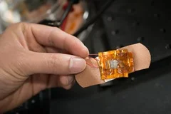
Zhenan Bao, a professor of chemical engineering at Stanford, has developed a heart monitor thinner than a dollar bill and no wider than a postage stamp. The flexible skin-like monitor, worn under an adhesive bandage on the wrist, is sensitive enough to help doctors detect stiff arteries and cardiovascular problems.

The devices could one day be used to continuously track heart health and provide doctors a safer method of measuring a key vital sign for newborn and other high-risk surgery patients.

Read More >>

Get free daily email updates!

Follow us!

Thursday, 28 February 2013

French researchers print first ADC on plastic

2013_0225_EE Millions of tons of food are wasted annually because 'the date'. But the date on the package is always a conservative estimate, so much food that is still good in the waste lands. Would it not be useful if the pack 'taste' of the food is still good? Researchers at the CEA-Liten, Eindhoven University of Technology, STMicroelectronics and University of Catania presented last week in the U.S. technical capstone that makes this possible - a plastic analogue to-digital converter. This gives a plastic sensor circuit of less than one euro cent feasible, which is an acceptable price increase is for example, a bag of potato chips or a piece of meat. The ultra cheap plastic electronics has many potential applications, for example in medicine.

“Organic electronics is still in its infancy, thus only simple digital logic and analogue functions have been demonstrated yet using printing techniques,” said CEA-Liten.

The ADC circuits printed by CEA-Liten include more than 100 n- and p-type transistors and a resistive layer on a transparent plastic sheet. The ADC circuit offers a resolution of 4 bits and has a speed of 2Hz.

The carrier mobility of the printed transistors is higher than the one observed in amorphous silicon, which is widely used in the display industry (CEA technology p-type µp = 1.8 cm²/V.s and n-type µn = 0.5 cm²/V.s).

Read more

Get free daily email updates!

Follow us!

Sunday, 24 February 2013

6 Ways to Improve Chip Yield Even Before the Project Starts

13782587-bulb-on-computer-chip--technology-concept Early on in Chip projects, yield is not taken very seriously. The common thinking goes –  anyhow there isn’t much to do as this early point of time. However, there are actually several things you can do even before the Chip design starts, which will translate to clear savings.

1- Know your Yield

Yield has a great deal of impact only if production volume is high. If you plan to manufacture only a few tens of thousands of components, perhaps yield is not the most important topic in your project’s plan.

Yield can be roughly calculated or estimated before the project has even started. Yet, if you have calculate a yield target of 95% there is no reason to invest money and efforts to try improving the yield from (the calculated) 95% to 99% because that would not be possible.  Therefore, it is important that you have calculated your yield and set that as a goal.

2- Consider Foundry Applicability

Semiconductor foundries are not taking any yield losses. It is not the fab responsibility whether your yield is high or low because they sell wafers and not dies. Therefore you should select the foundry the suits best to your Chip domain.

If you chip requires small node geometries go to GLOBALFOUNDRIES, TSMC etc. If you chip needs excellent RF performance go to: IBM, TowerJazz etc. The foundry can help you calculating the wafer yield based on their own process technology. If you can provide them with die size, number of layers, process node and options, they should be able to provide you with a very accurate yield figures for your project.

3- Match Design Team Experience to Your Project

If you have decided to outsource the frond-end and physical design activities to an external vendor, the main yield-related risk here is experience. If the design team does not have the relevant experience that matches your chip project (for instance: RF, High Voltage) you are really wasting your time. Don’t hire analog designer without high voltage experience if you need to design a 120V chip.

4- Select Silicon Proven IPs

More and more companies are shopping for Semiconductor IPs to help reduce time to market and minimize engineering cost. There are many IP vendors with high quality products and some with lower quality. The keyword here is risk minimization. You really want to make sure the IP blocks you are about to purchase and integrate into your chip are bug free and have been silicon proven and qualified for your process. Ask for test results and references.

5- Follow Package Design Rules

For simple QFN packages there are no real concerns besides following the assembly house design rules. However complex packages can reduce yield dramatically. If your chip uses a package that consists of a multilayer substrate with high speed signals, this substrate should be considered as part of the silicon die. Improper routing of high speed signals, for example, will make the substrate performance very marginal and thus result in failures during final test.

6 – Say No to Tight Test Limits, Say Yes to Better Hardware

The only place to measure yield is at the testing phase. And this is done by the ATE.

Great ASIC engineers often try to over-engineer the chip design and as a by-product also tighten up the test result criteria. These limits will have direct impact on your profit. Every device that fails to meet limits during the screening process will be scraped. Therefore, don’t create the perfect test specification. Make one that meets your system requirements.

Loadboards, sockets and probecards have different quality levels and therefore different cost. But since these are the actual physical interface between your chip and the tester, you want to make sure they have the right quality and durably to allow solid connectivity to the tester during the test period. Otherwise, lower quality hardware will shave off your yield figures. Sockets for example, have limited number of insertions; you therefore should buy a socket that meets your chip production volume. Bottom-line — don’t compromise on the quality of the hardware interfacing your chip.

There is so much more to write on this topic, we promise to write more articles in the future. Stay tuned.

Get free daily email updates!

Follow us!

Sunday, 10 February 2013

FPGAs: An Alternative To Cloud Computing !!

As complexity intensifies within sophisticated computing, so does the demand for more computing power. On top of that, the need to mine data from the burgeoning mountain of Internet search data has led to huge data centers that must be located close to water to feed their massive equipment cooling systems.

Weather modeling, for instance, continues to drill down into smaller geographical elements to fine-tune accuracy. And longer and more sophisticated encryption keys require greater compute power to crack them.

New tasks are also emerging in fields ranging from advertising to gene sequencing. Companies in the bio-sciences area gain competitive advantage based on the speed they’re able to sequence the genes held in DNA samples. Drug companies rely heavily on computer modeling to identify suitable candidate chemical formulas that may be useful in combating diseases.

In security, the focus has turned to deep packet inspection and application-aware monitoring. Companies now routinely deploy firewalls that are able to break into individual communication streams and identify traffic specific to, say, social networking sites, which can be used to help stop malicious attacks on corporate assets.

The Server Farm Approach

Traditionally, increases in processing requirements are handled with a brute force approach: Develop server farms that simply throw more microprocessor units at a problem. The heightened clamor for these server farms creates new problems, though, such as how to bring enough power to a server room and how to remove the generated heat. Space requirements are another problem, as is the complex management of the server farm to ensure factors like optimal load balancing, in terms of guaranteeing return on investment.

At some point, the rationale for these local server farms runs out as the physical and heat problems become too large. Enter the great savior to these problems, otherwise known as “The Cloud.” In this model, big companies will hire out operating time on huge computing clusters.

In a stroke, companies can make physical problems disappear by offloading this IT requirement onto specialised companies. However, it’s not without problems:

  • Depending on the data, there may be a requirement for high-bandwidth communications to and from the data centre.
  • A third party is added into the value chain, and it will try to make money out of the service based on used computing time.
  • Rather than solving the power problem, it’s simply been moved—exactly the same amount of computing needs to be undertaken, just in a different place.

This final issue, which raises fundamental problems that can’t be solved with traditional processor systems, splits into two parts:

  • Software: Despite advances in software programming tools, optimization of algorithms for execution on multiple processors is still far away. It’s often easy to break down a problem into a number of parallel computations. However, it’s much harder for the software programmer to handle the concept of pipelining, where the output of one stage of operation is automatically passed to the next stage and acted upon. Instead, processors perform the same operation on a large array of data, pass it to memory, and then call it back from memory to perform the next operation. This creates a huge overhead on power consumption and execution time.
  • Hardware: Processor systems are designed to be general. A processor’s data path is typically 32 or 64 bits. The data often requires much smaller resolution, leading to large inefficiencies as gates are clocked unnecessarily. Frequently, it becomes possible to pack data to fill more of the available data width, although this is rarely optimal and adds its own overhead. In addition, the execution units of a processor aren’t optimised to the specific mathematical or data-manipulation functions being undertaken, which again leads to huge overheads. 

The FPGA Approach

In the world of embedded products, a common computing-power approach is to develop dedicated hardware in an FPGA. These devices are programmed using silicon design techniques to implement processing functions much like a custom-designed chip. Many papers have been written on the relative improvements between processors, FPGAs, and dedicated hardware. Typical speed/power-consumption improvements range between a factor of 100 and 5000. 

Following in that vein, a recent study performed by Plextek explored how a single FPGA could accelerate a particular form of gene sequencing. Findings revealed an increase of just under a factor of 500. This can be viewed either as a significantly shorter time period or as an equipment reduction from 500 machines to a single PC. In reality, though, the savings will be a balance of the two.

Previously, these benefits were difficult to achieve for two reasons:

  • Interfacing: Dedicated engineering was required to develop FPGA systems that could easily access data sets. Once the data set changes, new interfacing requirements arise, which means a renewed engineering effort.
  • Design cycle time: The time it takes for an algorithm engineer to explain his requirements to a digital design engineer, who must then convert it all into VHDL along with the necessary testbenches to verify the design, simply becomes too long for exploratory algorithm work.

Now both of these problems have largely been solved thanks to modern FPGA devices. The first issue is resolved with embedded processors in the FPGA, which allow for more flexible interfacing. It’s even possible to directly access FPGA devices via Ethernet or even the Internet. For example, Plextek developed FPGA implementations that don’t have to go through interface modifications any time a requirement or data set changes.

To solve the second problem, companies such as Plextek have been working closely with major FPGA manufacturers to exploit new toolsets that can convert algorithmic descriptions defined in high-level mathematical languages (e.g., Matlab) into a form that easily converts into VHDL. As a result, significant time is saved from developing extensive testbenches to verify designs. Although not completely automatic, the design flow becomes much faster and much less prone to errors.

This doesn’t remove the need for a hardware designer, although it’s possible to develop methodologies to enable a hierarchical approach to algorithm exploration. The aim is to shorten the time between initial algorithm development and final solution.

Much of the time spent during algorithm exploration involves running a wide set of parameters through essentially the same algorithm. Plextek came up with a methodology that speeds up the process by providing a parameterised FPGA platform early in the process (see the figure). The approach requires the adoption of new high-level design tools, such as Altera’s DSP Builder or Xilinx’s System Generator.

74316_fig

A major portion of time involved in algorithm exploration revolves around running a wide set of parameters through essentially the same algorithm. Plextek’s methodology provides a parameterized FPGA platform early in the process, which saves a significant amount of time.

A key part of the process is jointly describing the algorithm parameters that are likely to change. After they’re defined, the hardware designer can deliver a platform with super-computing power to the scientist’s local machine, one that’s tailored to the algorithm being studied. At this point, the scientist can very quickly explore parameter changes to the algorithm, often being able to explore previously time-prohibitive ideas. As the algorithm matures, some features may need updating. Though modifications to the FPGA may be required, they can be implemented much faster.

A side benefit of this approach is that the final solution, when achieved, is in a hardware form that can be easily scaled across a business. In the past, algorithm exploration may have used a farm of 100 servers, but when rolled out across a business, the server requirements could increase 10- or 100-fold, or even to thousands of machines.  With FPGAs, equipment requirements will experience an orders-of-magnitude reduction.

Ultimately, companies that adopt these methodologies will achieve significant cost and power-consumption savings, as well as speed up their algorithm development flows.


Get free daily email updates!

Follow us!

Wednesday, 30 January 2013

Rambus Introduces R+ LPDDR3 Memory Architecture Solution

Virtium-DDR3-VLP-SO-UDIMM2 Sunnyvale, California, United States - January 28, 2013   – Rambus Inc. the innovative technology solutions company that brings invention to market, today announced its first LPDDR3 offering targeted at the mobile industry. In the Rambus R+ solution set, the R+ LPDDR3 memory architecture is fully compatible with industry standards while providing improved power and performance. This allows customers to differentiate their products in a cost-effective manner with improved time-to-market. Further helping improve design and development cycles, the R+ LPDDR3 is also available with Rambus’ collaborative design and integration services.

The R+ LPDDR3 architecture includes both a controller and a DRAM interface and can reduce active memory system power by up to 25% and supports data rates of up to 3200 megabits per second (Mbps), which is double the performance of existing LPDDR3 technologies. These improvements to power efficiency and performance enable longer battery life and enhanced mobile device functionality for streaming HD video, gaming and data-intensive apps.

“Each generation of mobile devices demands even higher performance with lower power. The R+ LPDDR3 technology enables the mobile market to use our controller and DRAM solutions to provide unprecedented levels of performance, with a significant power savings,” said Kevin Donnelly, senior vice president and general manager of the Memory and Interface Division at Rambus. “Since this technology is a part of our R+ platform, beyond the improvements in power and performance, we’re also maintaining compatibility with today’s standards to ensure our customers have all the benefits of the Rambus’ superior technology with reduced adoption risk.”

The seed to the improved power and performance offered by the R+ LPDDR3 architecture is a low-swing implementation of the Rambus Near Ground Signaling technology. Essentially, this single-ended, ground-terminated signaling technology allows devices to achieve higher data rates with significantly reduced IO power. The R+ LPDDR3 architecture is built from ground up to be backward compatible with LPDDR3 supporting same protocol, power states and existing package definitions and system environments.

Additional key features of the R+ LPDDR3 include:

  • 1600 to 3200Mbps data rates
  • Multi-modal support for LPDDR2, LPDDR3 and R+ LPDDR3
  • DFI 3.1 and JEDEC LPDDR3 standards compliant
  • Supports package-on-package and discrete packaging types
  • Includes LabStation™ software environment for bring-up, characterization, and validation in end-user application
  • Silicon proven design in GLOBALFOUNDRIES 28nm-SLP process

Get free daily email updates!

Follow us!

India fab decision likely this quarter

intro-fab BANGALORE, India—A decision on the long-pending proposal to set up a domestic wafer fab in India is likely to be made by the end of March, semiconductor industry executives said.
India has been debating building a wafer fab for years. A decision on whether to move forward with a plan to build a fab here had been promised by the end of 2012. But that deadline came and went with no decision made.

Still, semiconductor industry executives here said they are now far more confident that a decision on the plan by India's national government is imminent. Their optimism is based on some policies conducive to domestic electronics manufacturing being adopted last year, with still others in the works.

"Electronics manufacturing is being looked at more progressively," a representative of the India Semiconductor Association (ISA) said here Tuesday (Jan. 22).

A study conducted by the ISA and market researcher Frost & Sullivan on this market projected a compound annual growth rate of nearly 10 percent for India's electronics, system design and manufacturing market from 2011 through 2015. The market is expected to grow to $94.2 billion in 2015 from $66.6 billion in 2011, according to the study.

"This is a fantastic growth rate and should show the way to product development and value-added manufacturing domestically, rather than relying on imports and low value-added screwdriver assembly," the ISA said.

Fears loom over the import bill for electronic products though, with 65 percent of India's demand currently being met by imports.

Another worry is the projected decline in high value-added manufacturing within the country. Of the total electronics market of $44.81 billion in 2012, high value-added domestic manufacturing was just $3.55 billion. The ISA is concerned that this decline in high value-manufacturing will cause a cumulative opportunity loss of a whopping $200 billion by 2015.

India’s semiconductor market revenue was an estimated $6.54 billion in 2012. The country's semiconductor design industry is expected to grow at a 17 percent CAGR, amounting to over $10 billion in 2012. Of this, VLSI design accounted for $1.33 billion, embedded software for $8.58 billion and board/hardware design for $672 million.

Get free daily email updates!

Follow us!

Wednesday, 23 January 2013

IHS iSuppli: IC inventories hit record levels in Q3

hip inventories reached record highs near the end of 2012, and according to IHS iSuppli, semiconductor revenue will decline in Q1, prompting new concerns about the state of the market.

Overall semiconductor revenue is expected to slide three percent between January and March 2013, on top of a 0.7 percent decline in Q4 2012. What's more, inventory reached record levels in Q3 2012, amounting to 49.3 percent of revenue, more than at any point since Q1 2006. IHS iSuppli believes the uncomfortably high level of inventory points to the failure of key demand drivers to materialize.

The PC market remains slow and hopes of a Windows 8 renaissance have turned into a nightmare. Bellwether Intel saw its revenue drop three percent in Q4, with profit tumbling 27 percent, and the trend is set to continue. AMD is expected to announce its earnings Tuesday afternoon and more gloom is expected across the board. The only bright spot in an otherwise weak market is TSMC, which quickly rebounded after posting the lowest revenues in two years a year ago. TSMC now expects to see huge demand for 28nm products in 2013 and many observers point to a possible deal with Apple.

In addition, TSMC plans to invest $9 billion in capital expenditure in 2013, and it will likely spend even more in 2014, as it moves to ramp up 20nm production. However, Intel's plans to increase capital spending to $13 billion, up $2 billion over 2012 levels, have not been welcomed by analysts and investors. Unlike TSMC, Intel is not investing to increase capacity in the short term, it is making a strategic bet on 450mm wafer technology, which promises to deliver significantly cheaper chips compared to existing 300mm wafers. However, 450mm plants are still years away.

TSMC's apparent success has a lot to do with high demand for Smartphone's and tablets, which are slowly eating into the traditional PC market. Semiconductor shipments for the wireless segment were expected to climb around four percent in 2012 and positive trends were visible in analog, logic and NAND components. However, the mobile boom can't last forever, and we are already hearing talk of "Smartphone fatigue" and "peak Apple".

IHS iSuppli estimates the first quarter of 2013 will see growth in industrial and automotive electronics and other semiconductor markets will eventually overcome the seasonal decline, so a rebound is expected in the second and third quarters.

Semiconductor revenue could grow by four percent in the second, and nine percent in the third quarter. However, the assumptions are based on a wider economic recovery, which is anything but certain at this point. If demand evaporates, semiconductor suppliers could find themselves hit by an oversupply situation, leading to more inventory write-downs throughout the year.

Get free daily email updates!

Follow us!