Featured post

Top 5 books to refer for a VHDL beginner

VHDL (VHSIC-HDL, Very High-Speed Integrated Circuit Hardware Description Language) is a hardware description language used in electronic des...

Thursday, 31 May 2012

8-bit Micro Processor

This is 8-bit microprocessor with 5 instructions. It is based on 8080 architecture. This architecture called SAP for Simple-As-Possible computer. It very useful design which introduces most of the basic and fundamental ideas behind computer operation.

This design could be used for instruction classes for undergraduate classes or specific VHDL classes. This processor is based on the 8080 architecture, therefore, it could be upgraded step by step to integrate further facilities. It is very exciting challenge for the students to do so. Further, they could think about building complete system, i.e. integrating and I/O peripherals to the processor.

The design is proven for ASIC and FPGA. It was implemented using Xilinx FPGA Spartan-3E starter kit. A full documentation for the code and the used resources are attached within the project.

For project details please write to us on info@vlsiencyclopedia.com

Get free daily email updates!

Follow us!

Floating Point Adder and Multiplier

The FP Adder is a single-precision, IEEE-754 compliant, signed adder/substractor. It includes both single-cycle and 6-stage pipelined designs. The design is fully synthesizable and has been tested in a Xilinx Virtex-II XC2V3000 FPGA, occupying 385 CLBs and with a theoretical maximum operating frequency of 6MHz for the single-cycle design and 87MHz for the pipelined design. The design was tested at 33MHz.

The FP Multiplier is a single-precision, IEEE-754 compliant, signed multiplier. It includes both single-cycle and 4-stage pipelined designs. The design is fully synthesizable and has been tested in a Xilinx Virtex-II XC2V3000 FPGA, occupying 119 CLBs and with a theoretical maximum operating frequency of 8MHz for the single-cycle design and 90MHz for the pipelined design. The design was tested at 33MHz.

Features

- IEEE-754 compliant
- 32 bits, single precision
- Works with normalized and un-normalized numbers
- Simple block design, good for FP arithmetic learning
- Adder
- 385 CLBs
- 87 MHz, 6-stage pipelined
- Multiplier
- 119 CLBs
- 90 MHz, 4-stage pipelined

PROGRESSIVE CODING FOR WAVELET-BASED IMAGE COMPRESSION

Description of the Project:-

This paper describes the hardware design flow of lifting based 2-D Forward Discrete Wavelet Transform (FDWT) processor for JPEG 2000. In order to build high quality image of JPEG 2000 codec, an effective 2-D FDWT algorithm has been performed on input image file to get the decomposed image coefficients. The Lifting Scheme reduces the number of operations execution steps to almost one-half of those needed with a conventional convolution approach. Initially, the lifting based 2-D FDWT algorithm has been developed using Mat lab. The FDWT modules were simulated using XPS(8.1i) design tools. The final design was verified with Matlab image processing tools.

Comparison of simulation results Matlab was done to verify the proper functionality of the developed module. The motivation in designing the hardware modules of the FDWT was to reduce its complexity, enhance its performance and to make it suitable development on a reconfigurable FPGA based platform for VLSI implementation. Results of the decomposition for test image validate the design. The entire system runs at 215 MHz clock frequency and reaches a speed performance suitable for several realtime applications. The result of simulation displays that lifting scheme needs less memory requirement.

Introduction :
A majority of today’s Internet bandwidth is estimated to be used for images and video. Recent multimedia applications for handheld and portable devices place a limit on the available wireless bandwidth. The bandwidth is limited even with new connection standards. JPEG image compression that is in widespread use today took several years for it to be perfected. Wavelet based techniques such as JPEG2000 for image compression has a lot more to offer than conventional methods in terms of compression ratio. Currently wavelet implementations are still under development lifecycle and are being perfected. Flexible energy-efficient hardware implementations that can handle multimedia functions such as image processing, coding and decoding are critical, especially in hand-held portable multimedia wireless devices.

Background
Data compression is, of course, a powerful, enabling technology that plays a vital role in the information age. Among the various types of data commonly transferred over networks, image and video data comprises the bulk of the bit traffic. For example, current estimates indicate that image data take up over 40% of the volume on the Internet. The explosive growth in demand for image and video data, coupled with delivery bottlenecks has kept compression technology at a premium.
Among the several compression standards available, the JPEG image compression standard is in wide spread use today. JPEG uses the Discrete Cosine Transform (DCT) as the transform, applied to 8-by-8 blocks of image data. The newer standard JPEG2000 is based on the Wavelet Transform (WT). Wavelet Transform offers multi-resolution image analysis, which appears to be well matched to the low level characteristic of human vision. The DCT is essentially unique but WT has many possible realizations. Wavelets provide us with a basis more suitable for representing images.

This is because it cans represent information at a variety of scales, with local contrast changes, as well as larger scale structures and thus is a better fit for image data.

Aim of the project
The main aim of the project is to implement and verify the image compression technique and to investigate the possibility of hardware acceleration of DWT for signal processing applications. A hardware design has to be provided to achieve high performance, in comparison to the software implementation of DWT. The goal of the project is to

. Implement this in a Hardware description language (Here VHDL).
. Perform simulation using tools such as Xilinx ISE 8.1i.
. Check the correctness and to synthesize for a Spartan 3E FPGA Kit.

The STFT represents a sort of compromise between the time- and frequency-based views of a signal. It provides some information about both when and at what frequencies a signal event occurs. However, you can only obtain this information with limited precision, and that precision is determined by the size of the window.

While the STFT compromise between time and frequency information can be useful, the drawback is that once you choose a particular size for the time window, that window is the same for all frequencies. Many signals require a more flexible approach—one where we can vary the window size to determine more accurately either time or frequency.

Problem Present in Fourier Transform : The Fundamental idea behind wavelets is to analyze according to scale. Indeed, some researchers feel that using wavelets means adopting a whole new mind-set or perspective in processing data. Wavelets are functions that satisfy certain mathematical requirements and are used in representing data or other functions. This idea is not new. Approximation using superposition of functions has existed since the early 18OOs, when Joseph Fourier discovered that he could superpose sines and cosines to represent other functions.

However, in wavelet analysis, the scale used to look at data plays a special role. Wavelet algorithms process data at different scales or resolutions. Looking at a signal (or a function) through a large “window,” gross features could be noticed. Similarly, looking at a signal through a small “window,” small features could be noticed. The result in wavelet analysis is to see both the forest and the trees, so to speak.

This makes wavelets interesting and useful. For many decades scientists have wanted more appropriate functions than the sines and cosines, which are the basis of Fourier analysis, to approximate choppy signals.’ By their definition, these functions are non-local (and stretch out to infinity). They therefore do a very poor job in approximating sharp spikes. But with wavelet analysis, we can use approximating functions that are contained neatly in finite domains. Wavelets are well-suited for approximating data with sharp discontinuities.

The wavelet analysis procedure is to adopt a wavelet prototype function, called an analyzing wavelet or mother wavelet. Temporal analysis is performed with a contracted, high-frequency version of the prototype wavelet, while frequency analysis is performed with a dilated, low-frequency version of the same wavelet. Because the original signal or function can be represented in terms of a wavelet expansion (using coefficients in a linear combination of the wavelet functions), data operations can be performed using just the corresponding wavelet coefficients.

And if wavelets best adapted to data are selected, the coefficients below a threshold is truncated, resultant data are sparsely represented. This sparse coding makes wavelets an excellent tool in the field of data compression. Other applied fields that are using wavelets include astronomy, acoustics, nuclear engineering, sub-band coding, signal and image processing, neurophysiology, music, magnetic resonance imaging, speech discrimination, optics, fractals, turbulence, earthquake prediction, radar, human vision, and pure mathematics applications such as solving partial differential equations.

Basically wavelet transform (WT) is used to analyze non-stationary signals, i.e., signals whose frequency response varies in time, as Fourier transform (FT) is not suitable for such signals. To overcome the limitation of FT, short time Fourier transform (STFT) was proposed. There is only a minor difference between STFT and FT. In STFT, the signal is divided into small segments, where these segments (portions) of the signal can be assumed to be stationary. For this purpose, a window function "w" is chosen. The width of this window in time must be equal to the segment of the signal where its still be considered stationary. By STFT, one can get time-frequency response of a signal simultaneously, which can’t be obtained by FT.

Scaling
We’ve seen the interrelation of wavelets and quadrature mirror filters. The wavelet function  is determined by the high pass filter, which also produces the details of the wavelet decomposition.
There is an additional function associated with some, but not all wavelets. This is the so-called scaling function. The scaling function is very similar to the wavelet function. It is determined by the low pass quadrature mirror that iteratively up- sampling and convolving the high pass filter produces a shape approximating the wavelet function, iteratively up-sampling and convolving the low pass filter produces a shape approximating the scaling function.We’ve already alluded to the fact that wavelet analysis produces a time-scale view of a signal and now we’re talking about scaling and shifting wavelets.

What exactly do we mean by scale in this context?
Scaling a wavelet simply means stretching (or compressing) it. To go beyond colloquial descriptions such as “stretching,” we introduce the scale factor, often denoted by the letter a.

If we’re talking about sinusoids, for example the effect of the scale factor is very easy to see:

One-Stage Decomposition
For many signals, the low-frequency content is the most important part. It is what gives the signal its identity. The high-frequency content on the other hand imparts flavor or nuance. Consider the human voice. If you remove the high-frequency components, the voice sounds different but you can still tell what’s being said. However, if you remove enough of the low-frequency components, you hear gibberish. In wavelet analysis, we often speak of approximations and details. The approximations are the high-scale, low-frequency components of the signal. The details are the low-scale, high-frequency components. The filtering process at its most basic level looks like this:

The original signal S passes through two complementary filters and emerges as two signals. Unfortunately, if we actually perform this operation on a real digital signal, we wind up with twice as much data as we started with. Suppose, for instance that the original signal S consists of 1000 samples of data. Then the resulting signals will each have 1000 samples, for a total of 2000. These signals A and D are interesting, but we get 2000 values instead of the 1000 we had. There exists a more subtle way to perform the decomposition using wavelets.

RISC Processor

A small RISC CPU (written in VHDL) that is compatible with the 12 bit opcode PIC family. Single cycle operation normally, two cycles when the program counter is modified. Clock speeds of over 40Mhz are possible when using the Xilinx Virtex optimizations.
Licensed under LGPL.

The core has a single pipeline stage and is run from a single clock, so (ignoring program counter changes) a 40Mhz clock will give 40 MIPS processing speed. Any instruction which modifies the program counter, for example a branch or skip, will result in a pipeline stall and this will only cost one additional clock cycle.

The CPU architecture chosen is not particularly FPGA friendly, for example multiplexers are generally quite expensive. The maximum combinatorial path delay is also long, so to ease the place and route tool's job the core is written at a low level. It instantiates a number of library macros, for example a 4:1 mux. Two versions of these are given, one is generic VHDL and the second is optimized for Xilinx Virtex series (including Spartan devices).

Sunday, 27 May 2012

Dual Edge D-FlipFlop

One important design rule is to use only one edge of the clock signal. Although this is a good design practice in some special cases it might be helpful to use both edges.

Fig-1Fig. 1

Listing 1. not synthesizable dual-edge behavior in VHDL

process (reset, clock)
begin
if (reset =  ‘1’) then
−− reset
elsif rising_edge(clock) then
−− synchronous behavior
elsif falling_edge (clock) then
−− synchronous behavior
end if;
end process;

One example is low-power signal processing, where all state machines should run at the symbol frequency to avoid unnecessary switching. But the signal frequency might be higher than the symbol frequency.
FM0 encoding (fig. 1) is an example. With FM0 encoding always the signal switches at the begin of every symbol. Another signal switch is done in the middle of the symbol, if zero has to be transmitted. If a transmitter wants so send a FM0 encoded data stream and runs only at the symbol frequency, the output signal has to be switched with the rising edge of clock and additionally with the falling edge, if zero is transmitted.

Another example for dual-edge behavior are clock dividers. For odd divisors the divided clock signal has to be switched at the falling edge of the fast clock, to get the same length for the low and the high period.

There are two problems if dual-edge behavior is desired:

  1. Most cell libraries do not provide a dual-edge flip-flops.
  2. In VHDL dual-edge behavior can be described as shown in listing 1, but most synthesis tools do not support this. Only few are capable of handling such a description. Therefore we need another way to model dual-edge behavior.

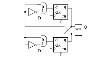
Although dual-edge behavior is not supported by VHDL, synthesis and the cell libraries, a dual-edge flipflop can be described as shown in fig. 2. Note that synthesis tools will transform the multiplexers into XOR gates.

image Fig. 2. Pseudo Dual-Edge D-Flipflop (pde dff)

The pde dff consists of 2 cross-coupled flipflops, one triggered by the rising and the other one triggered by the falling edge of the clock signal c. The outputs of the flipflops are connected via an XOR gate. Although not shown in fig. 2, asynchronous set and reset are possible.

The synthesizable VHDL source code of the pde dff is shown in listing 2. Both asynchronous set (sn) and reset (rn) can be turned on or off using generic parameters. Using both edges of the clock means doubling the clock frequency. Propagation paths have to be half as long for dualedge logic compared to common single-edge logic.

Although the pde dff looks symmetric it has in general asymmetric behavior in terms of the propagation time for the rising and the falling edge of the data output q. It depends on the data input d, the stored values in the two flip-flops and the propagation times of both the flip-flops and the final XOR gate.

For the example of FM0 encoding (fig. 1) this means that for a continuous transmission of the symbol zero in general the time of the output q being high is not equal to the time of the output being low. Such an asymmetry is not uncommon even for single-edge flipflops but for the pde dff it is slightly bigger.

Listing2. The Pseudo Dual-Edge D-FF in VHDL:

library IEEE;
use IEEE.STD_LOGIC_1164.ALL;
IEEE.Numeric_std.ALL;

entity pdedff is
generic (
impl_rn: integer := 1; −− with async reset if 1
impl_sn: integer := 1); −− with async set if 1
port(
rn:in std_ulogic; −− low−active
sn:in std_ulogic; −− low−active
d:in std_ulogic;
c:in std_ulogic;
q:out std_ulogic);
end pdedff;

−−pseudo dual−edgeD−flipflop
−−reset and set are lowactive and can be
−−(de)activated using the generic paramters

architecture behavior of pdedff is
signal ff_rise, ff_fall:std_ulogic;
begin

process(rn, sn, c)
begin
if(impl_rn=1 AND rn=’0’) then
ff_rise <= ’0’;
elsif (impl_sn=1 AND sn=’0’) then
ff_rise <= ‘1’;
elsif rising_edge (c) then
if (d= ‘1’) then
ff_rise <= NOT (ff_fall);
else ff_rise <= ff_fall;
endif;
endif;
end process;

process(rn, sn, c)
begin
if(impl_rn = 1 AND rn= ‘0’) then
ff_fall <= ‘0’;
elsif (impl_sn= 1 AND sn = ‘0’) then
ff_fall <= ‘0’;
elsif falling_edge (c) then
if (d = ‘1’) then
ff_fall <= NOT (ff_rise);
else
fffall <= ff_rise;
endif;
endif;
end process;

q <= ‘0’ when (impl_rn = 1 AND rn= ‘0’) else
        ‘1’ when (impl_sn= 1 AND sn= ‘0’) else
        ff_rise XOR ff_fall;
−−rn and sn used to suppress spikes
endbehavior;

45nm 32 nm 28nm 24nm 22nm ….. What Does It Mean?

Intel's new microprocessor relies on a new recipe that combines the element Hafnium and metal gate technology to increase performance and significantly reduce eco-unfriendly, wasteful electricity leaks. But what does that mean?


Semiconductor manufacturing processes

  • 10 µm — 1971
  • 3 µm — 1975
  • 1.5 µm — 1982
  • 1 µm — 1985
  • 800 nm (.80 µm) — 1989
  • 600 nm (.60 µm) — 1994
  • 350 nm (.35 µm) — 1995
  • 250 nm (.25 µm) — 1998
  • 180 nm (.18 µm) — 1999
  • 130 nm (.13 µm) — 2000
  • 90 nm — 2002
  • 65 nm — 2006
  • 45 nm — 2008
  • 32 nm — 2010
  • 22 nm — 2011
  • 16 nm — approx. 2013
  • 11 nm — approx. 2015
  • 6 nm — approx. 2020
  • 4 nm — approx. 202

Friday, 11 May 2012

ZeroN project, Computer-controlled magic levitation created by MIT student

What if materials could defy gravity, so that we could leave them suspended in mid-air?

MIT genius Jinha Lee has created an incredible computer-controlled system for levitating objects.

The project, called ZeroN, uses magnets, a Kinect visual system, plus special software that enables either the computer to move a steel ball around in space, or a human to just grab it and move it, essentially telling the computer where it should go.

ZeroN is a new physical/digital interaction element that can be levitated and moved freely by computer in a three dimensional space. Both the computer and people can move the ZeroN simultaneously. In doing so, people and computers can physically interact with one another in 3D space.

It can even remember how it was moved, then repeat the movement automatically.

I really want to experience it live …!!

http://www.leejinha.com/zeron

http://web.media.mit.edu/~jinhalee/zeron_jinha_lee.pdf

Tuesday, 8 May 2012

Xilinx introduces Vivado Design Suite

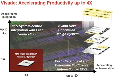
Xilinx Inc. has announced the Vivado Design Suite. It enables an IP and system centric next generation design environment. Especially meant for the next decade of ‘All-Programmable’ devices, it also accelerates the integration and implementation up to 4X. And, why now? That’s because the all-programmable devices enable programmable systems ‘integration.

Xilinx_VivadoThere are system integration bottlenecks, such as design and IP re-use, integrating algorithmic and RTL level IP, mixing DSP, embedded, connectivity and logic, and verification of blocks and “systems”.
There are implementation bottlenecks as well, such as hierarchical chip planning, multi-domain and multi-die physical optimization, predictable ‘design’ vs. ‘timing’ closure, and late ECOs and rippling effect of changes.
Vivado accelerates productivity up to 4X. The design suite elements include an integrated design environment, has a shared scalable data model, is scalable to 100 million gates, and debug and analysis. It shares design information between implementation steps that ensures fast convergence and timing closure. This enables highly efficient memory utilization. Also, it is scalable to future families, that are greater than 10 million logic cells (100 million gates) and enables cross-probing across the entire design.
Vivado also enables packaging designs into system-level IP for re-use. You can share IP within your team, project or company. Any 3rd party IP is delivered with a common look and feel. You can re-use IP at any point in the implementation process. The IP can be source, placed, or placed and routed.

Tips for an Error-free Functional Simulation

Getting a VHDL code to work in the functional simulation is not always an easy task.This article will cover some tips to quickly point out the errors in the code and make your life easier.

  1. Create a proper sensitivity list. Some times you may have to add other control signals too(other than clock) into you sensitivity list to get is working.
  2. Initialize the signals and variables correctly. If they are not initialized(normally they are set to '0'), then these signals will appear as "U"in the simulation waveform.
  3. If you see "X" in the waveform then that indicates concurrent writing to the same signal. A simple re-arrangement of the signal inside the process will normally take out this bug.
  4. In case you have arrays in the design make sure to check for out of bound error. This happens when you read or write a different index than the one available within the range of array.
  5. If elsif's are error prone. Always try to consider all the conditions of If elsif. If a particular condition is not considered then the value will remain unchanged. If you don’t want this to happen then make sure you reset the signal, using an else condition.
  6. Within a process, signal assignments can be written in any order. They will get executed concurrently. But for variables, the order matters. line 1 is executed first, line 2 second and so on...
  7. One way to debug the code is to force one or more signals as constants and test the design. This will help you in localizing the error.
  8. Writing a location in RAM requires a small time delay. Account for this, while reading and writing from the same location in the same clock cycle. The read data will be the one written in the last clock cycle.
  9. Try synthesizing the design. The synthesizer tool may give out some warnings or errors which will point you in the correct direction to solve the error in the functional simulation.
  10. When using components in the design, use name instantiation, so that you don't accidentally assign wrong signals to the component ports.

VHDL to Verilog to VHDL Code Converter Tools & Tips

Most modern EDA tools will accept both VHDL and Verilog, and even combination of the two in the same design. Even though engineers try to convert from VHDL to Verilog, or Verilog to VHDL in some cases depends on their requirement in design work flow.

Possible Reasons of Code Conversion Between VHDL and Verilog

  • To reuse existing designs
  • To maintain both version of a design. Verilog for commercial, industrial purposes and VHDL for DoD requirements.
  • To design, support the code for different countries like US, Europe and or Asia where preference for particular language differs.

As a general rule, it is better to write own coding in the targeted HDL such as VHDL or Verilog. However, the time you will spend on the “manual translation” could also be used to make a design on your own.

The commercially available code conversion/translation tools convert the code as module wise, and may not necessarily support every possible construct you can find in VHDL or Verilog.

In case of urgent need, the tools will help in translating the larger code from VHDL to Verilog (and Verilog to VHDL too) on the fly. Few of them are for command line use in UNIX environment, and a few are GUI enabled so that you can execute them in Windows.

VHDL to Verilog (Verilog to VHDL) Code Conversion Translation Tools

Here is the list of some popular Vendors, supply HDL code conversion tools. Few are free download, and others cost a little but gives a demo version with some limitation on code size.

  • Synapticad’s V2V Translation Tool, supports both VHDL to Verilog and vice versa
  • MyHDL, supports both VHDL to Verilog and vice versa
  • TauDelta’s Verilog to VHDL RTL converter
  • Trilent Networks HDL Translator
  • Alternate System Concepts Inc.
  • Avanti Corp.
  • Aldec Corporation’s Active-HDL
  • X-Tek Corporation’s XHDL
  • FTL Systems
  • Ocean Logic

Saturday, 5 May 2012

Teach SystemVerilog Yourself

SystemVerilog emerged a few years ago and has gained phenomenal popularity ever since. Today this language is virtually ubiquitous and all 3 big EDA vendors keep pushing it forward. So if you consider yourself a modern verifier, you'd better get familiar with SystemVerilog unless you want to stay in the dark.

While Think Verification focuses on the advanced stuff (check out our VMM Hacker's Guide series), there are many websites and blogs out there that offer free tutorials that can help you learn the basics of SystemVerilog.

Though we are going to cover all aspects of SystemVerilog in this site, We like to share with you some of the online available resources that you can refer. Here are a few links that will help you get started very quickly:

ASIC WORLD

A comprehensive tutorial that shows you most of the constructs and elements of the language. There's far more information than you need to get you through your first steps, but it's a good place to keep as reference. The examples given there also include snapshots from the simulator's output which is cool. Methodology is not covered there, although the author intends to cover that in the future.

DOULOS

Probably the first place to look. Doulos offers a sleek tutorial covering some of the most important elements of SystemVerilog in a nutshell. Although not comprehensive, we think their tutorial gives a nice overview of the language fundamentals that you should get familiar with, especially if you have experience in other HVLs. Their quick tutorial on Classes and Randomization will get you started rapidly.

ELECTRO-SOFTS

This tutorial covers the basic constructs of SystemVerilog quite thoroughly, along with some good examples. This might be a good place to go once you nail the basic concepts of the language. Methodology is not covered here but we liked their SVA (System Verilog Assertions) section.

TESTBENCH.IN

A comprehensive tutorial that covers all of SystemVerilog's fundamentals, including OOP and DPI. They also cover VMM quite well. There are a couple of labs for you to download if you're up for it. Overall - a great tutorial that teaches language as well as methodology.

SPECMAN-VERIFICATION

An evolving (and funny) tutorial on SystemVerilog that's quite different from the other "serious" looking tutorials out there. Avidan (the author) shares with us not only the basic constructs of SV but also his philosophical view on each one of them. Definitely worth a visit if you're into learning SystemVerilog. 

The 3 M's of Verification: Methodology! Methodology! Methodology!

SystemVerilog alone is not enough if you're serious about building verification environments. That's where standard methodology comes in. Today there are two main methodologies in the market for SystemVerilog. The first is VMM, the other is OVM. Both methodologies can do the job and there's plenty of information out there on each one of them. OVM-World and VMM-Central are probably the best places to start looking (pretty soon a new methodology is going to conquer the world - UVM, which is based on OVM plus parts of VMM). A word of advice - pay as much attention to methodology as you would to language constructs and syntax. In HVLs, and in SystemVerilog in particular, methodology accounts for the greater part of your verification project.