Featured post

Top 5 books to refer for a VHDL beginner

VHDL (VHSIC-HDL, Very High-Speed Integrated Circuit Hardware Description Language) is a hardware description language used in electronic des...

Showing posts with label Nanotechnology. Show all posts

Monday, 5 October 2015

IBM steps forward to replace Silicon Transistors with Carbon Nanotubes

Carbon Nanotube
Carbon Nanotube
The breakthrough is that - IBM improves carbon nanotube scaling below 10nm. How ever before calling it as breakthrough we should also check out what other giants like Intel, AMD, TSMC or Samsung is working on. This breakthrough has relation with the Moore's Law. Yes you got right..!!It says that the transistor counts double only every 18 month or so. It’s the time that Intel marks 40 years of the 4004 microprocessor and here now lying some fear that progress will soon hit a wall.

You can refer to my post History and Evolution of Integrated Circuits where it shows clear progress of semiconductor industry.

But not to worry, IBM has developed a way that could help the semiconductor industry continue to make ever more dense chips to support Moore's law. These chips will be both faster and more power efficient.

Few glimpse of carbon nanotube transistors

  • Carbon nanotube transistors can operate at ten nanometers
  • Equivalent to 10,000 times thinner than a strand of human hair
  • Less than half the size of today’s leading silicon technology
  • Could also mean wearables that attach directly to skin and internal organs


Here I have an animation for Animated Nanofactory in Action.

As a result of this the devices will become smaller, increased contact resistance for carbon nanotubes has hindered performance gains until now.

These results could overcome contact resistance challenges all the way to the 1.8 nanometer node – four technology generations away.

A project at IBM is now aiming to have transistors built using carbon nanotubes ready to take over from silicon transistors soon after 2020. According to the semiconductor industry’s roadmap, transistors at that point must have features as small as five nanometers to keep up with the continuous miniaturization of computer chips.

IBM has previously shown that carbon nanotube transistors can operate as excellent switches at channel dimensions of less than ten nanometers – the equivalent to 10,000 times thinner than a strand of human hair and less than half the size of today’s leading silicon technology.

IBM's new contact approach overcomes the other major hurdle in incorporating carbon nanotubes into semiconductor devices, which could result in smaller chips with greater performance and lower power consumption.

Earlier this summer, IBM unveiled the first 7 nanometer node silicon test chip, pushing the limits of silicon technologies and ensuring further innovations for IBM Systems and the IT industry.

By advancing research of carbon nanotubes to replace traditional silicon devices, IBM is paving the way for a post-silicon future and delivering on its $3 billion chip R&D investment announced in July 2014.

IBM’s chosen design uses six nanotubes lined up in parallel to make a single transistor. Each nanotube is 1.4 nanometers wide, about 30 nanometers long, and spaced roughly eight nanometers apart from its neighbors. Both ends of the six tubes are embedded into electrodes that supply current, leaving around 10 nanometers of their lengths exposed in the middle. A third electrode runs perpendicularly underneath this portion of the tubes and switches the transistor on and off to represent digital 1s and 0s.

The IBM team has tested nanotube transistors with that design, but so far it hasn't found a way to position the nanotubes closely enough together, because existing chip technology can’t work at that scale. The favored solution is to chemically label the substrate and nanotubes with compounds that would cause them to self-assemble into position. Those compounds could then be stripped away, leaving the nanotubes arranged correctly and ready to have electrodes and other circuitry added to finish a chip.

Sunday, 18 August 2013

Animated Nanofactory in Action


A nanofactory, as the name implies, is a device or system that can assemble products at molecular level.  Products of nanotechnology are already in our midst, but most of these are passive consumer products such as coating materials and pharmaceuticals.  Nanofactories that produce macroscopic active consumer products (such as laptops as depicted in this animation) will be in the realm of science fiction for two more decades.

We know, however, that the building blocks of these nanofactories someday are already here in the form of microelectromechanical systems, or MEMS, which are semiconductor devices with mechanical moving parts.  Today, MEMS applications include those in optical micromirrors for guided-wave optical switching applications and accelerometers for automotive airbag deployment systems, gaming console interfaces, etc.

Get free daily email updates!

Follow us!

Thursday, 27 June 2013

Quantum-tunneling technique

Quantum-tunneling technique promises chips that won't overheat

quantumpicResearchers at Michigan Technological University have employed room-temperature quantum tunneling to move electrons through boron nitride nanotubes. Semiconductor devices made with this technology would need less power than current transistors require, while also not generating waste heat or leaking electrical current, according to the research team.

Rather than relying on a predictable flow of electrons of current circuits, the new approach depends on quantum tunneling. In this, electrons travel faster than light and appear to arrive at a new location before having left the old one, and pass straight through barriers that should be able to hold them back. This appears to be under the direction of a cat which is possibly dead and alive at the same time, but we might have gotten that bit wrong.

here is a lot of good which could come out of building such a computer circuit. For a start, the circuits are built by creating pathways for electrons to travel across a bed of nanotubes, and are not limited by any size restriction relevant to current manufacturing methods.

Read more >>

Saturday, 18 May 2013

flexible heart monitor thinner than a dollar bill

12625-babyskin_news Stanford Engineers combine layers of flexible materials into pressure sensors to create a wearable heart monitor thinner than a dollar bill. The skin-like device could one day provide doctors with a safer way to check the condition of a patient's heart.

Most of us don't ponder our pulses outside of the gym. But doctors use the human pulse as a diagnostic tool to monitor heart health.

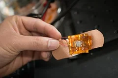
Zhenan Bao, a professor of chemical engineering at Stanford, has developed a heart monitor thinner than a dollar bill and no wider than a postage stamp. The flexible skin-like monitor, worn under an adhesive bandage on the wrist, is sensitive enough to help doctors detect stiff arteries and cardiovascular problems.

The devices could one day be used to continuously track heart health and provide doctors a safer method of measuring a key vital sign for newborn and other high-risk surgery patients.

Read More >>

Get free daily email updates!

Follow us!

Wednesday, 24 April 2013

UI scientists create powerful microbatteries

UI …. i.e. University of Illinois…

IonCrossing_in_new_battery Developed by researchers at the University of Illinois at Urbana-Champaign, the new microbatteries out-power even the best supercapacitors and could drive new applications in radio communications and compact electronics.

The most powerful batteries on the planet are only a few millimeters in size, yet they pack such a punch that a driver could use a cellphone powered by these batteries to jump-start a dead car battery – and then recharge the phone in the blink of an eye.

“This is a whole new way to think about batteries. A battery can deliver far more power than anybody ever thought. In recent decades, electronics have gotten small. The thinking parts of computers have gotten small. And the battery has lagged far behind. This is a microtechnology that could change all of that. Now the power source is as high-performance as the rest of it,” said William P. King, bliss professor of mechanical science and engineering.

“The picture illustrates a high power battery technology from the University of Illinois.  Ions flow between three-dimensional micro-electrodes in a lithium ion battery.”

With currently available power sources, users have had to choose between power and energy. For applications that need a lot of power, like broadcasting a radio signal over a long distance, capacitors can release energy very quickly but can only store a small amount. For applications that need a lot of energy, like playing a radio for a long time, fuel cells and batteries can hold a lot of energy but release it or recharge slowly.

The new microbatteries offer both power and energy, and by tweaking the structure a bit, the researchers can tune them over a wide range on the power-versus-energy scale.

The batteries owe their high performance to their internal three-dimensional microstructure. Batteries have two key components: the anode (minus side) and cathode (plus side). Building on a novel fast-charging cathode design by materials science and engineering professor Paul Braun’s group, King and Pikul developed a matching anode and then developed a new way to integrate the two components at the microscale to make a complete battery with superior performance.

The graphic illustrates a high power battery technology from the University of Illinois.  Ions flow between three-dimensional micro-electrodes in a lithium ion battery.

With so much power, the batteries could enable sensors or radio signals that broadcast 30 times farther, or devices 30 times smaller. The batteries are rechargeable and can charge 1000 times faster than competing technologies – imagine juicing up a credit-card-thin phone in less than a second. In addition to consumer electronics, medical devices, lasers, sensors and other applications could see leaps forward in technology with such power sources available.

“Any kind of electronic device is limited by the size of the battery – until now. Consider personal medical devices and implants, where the battery is an enormous brick, and it’s connected to itty-bitty electronics and tiny wires. Now the battery is also tiny,” explained Mr. King.

Now, the researchers are working on integrating their batteries with other electronics components, as well as manufacturability at low cost.

“To dare is to lose one's footing momentarily. To not dare is to lose oneself.”

Get free daily email updates!

Follow us!

Thursday, 28 February 2013

French researchers print first ADC on plastic

2013_0225_EE Millions of tons of food are wasted annually because 'the date'. But the date on the package is always a conservative estimate, so much food that is still good in the waste lands. Would it not be useful if the pack 'taste' of the food is still good? Researchers at the CEA-Liten, Eindhoven University of Technology, STMicroelectronics and University of Catania presented last week in the U.S. technical capstone that makes this possible - a plastic analogue to-digital converter. This gives a plastic sensor circuit of less than one euro cent feasible, which is an acceptable price increase is for example, a bag of potato chips or a piece of meat. The ultra cheap plastic electronics has many potential applications, for example in medicine.

“Organic electronics is still in its infancy, thus only simple digital logic and analogue functions have been demonstrated yet using printing techniques,” said CEA-Liten.

The ADC circuits printed by CEA-Liten include more than 100 n- and p-type transistors and a resistive layer on a transparent plastic sheet. The ADC circuit offers a resolution of 4 bits and has a speed of 2Hz.

The carrier mobility of the printed transistors is higher than the one observed in amorphous silicon, which is widely used in the display industry (CEA technology p-type µp = 1.8 cm²/V.s and n-type µn = 0.5 cm²/V.s).

Read more

Get free daily email updates!

Follow us!

Tuesday, 30 October 2012

IBM's New Chip Tech.

IBM Scientist holds bottles full of carbon nanotubes IBM has put the chip industry on notice by inventing a new technology that would replace silicon with a new material, carbon nanotubes.

IBM has found a new way to put what seems like an impossibly large number of transistors into an insanely small area, the width of only a few atoms. That's 10,000 times thinner than a strand of human hair and less than half the size of the leading silicon technology.

Or as IBM explains:

Carbon nanotubes are single atomic sheets of carbon rolled up into a tube. The carbon nanotube forms the core of a transistor device that will work in a fashion similar to the current silicon transistor, but will be better performing. They could be used to replace the transistors in chips that power our data-crunching servers, high performing computers and ultra fast smart phones.

Inventing the tech is one thing, being able to manufacture it at scale is another. And that's the real breakthrough IBM announced. It has put more than 10,000 of these "nano-sized tubes of carbon" onto single chip using a standard fabricating method.

It will still be years, maybe even a decade, before carbon nanotubes would really replace silicon-based chips in our servers and our smartphones. But this breakthrough is important because the chip industry is reaching a point where it physically can't squeeze much more processing power onto existing forms of chips.  Some have predicted that we'll soon reach an end to Moore's Law which tries to double the density of chips on a wafer every two years.

Chip transistors are already super tiny—or nanoscale.

ibm-carbon-nanotube

This is what a nanotube looks like under a microscope.

Earlier this year Intel dumped $4.1 billion into two new techniques to help the chip industry continue to get more powerful at smaller scales. These two new technologies are not the same as what IBM is working on.

IBM's carbon-based method may represent a whole new beginning for Moore's Law, the industry maxim that chips keep getting cheaper, more powerful, and smaller.

Monday, 30 July 2012

To 20nm and beyond: ARM targets Intel with TSMC collaboration

The multi-year deal sees ARM tie itself even closer to TSMC, its chip-fabber of choice, as it looks to capitalise on the company's technology to help it maintain a lead over Intel for chip power efficiency.

building-the-low-power-20nm-ecosystem ARM is ramping up its push to get its highly efficient low-power chips into servers by signing a multi-year agreement with Asian silicon manufacturer TSMC.
Under the deal, the Cambridge-based chip designer has agreed to share technical details with TSMC to help the fabricator make better chips with higher yields, ARM said on Monday. TSMC will also share information, so that ARM can create designs better suited to its manufacturing.

"By working closely with TSMC, we are able to leverage TSMC's ability to quickly ramp volume production of highly integrated SoCs [System-on-a-Chip processors] in advanced silicon process technology," Simon Segars, general manager for ARM's processor and physical IP divisions, said in a statement.

"The ongoing deep collaboration with TSMC provides customers earlier access to FinFET technology to bring high-performance, power-efficient products to market," he added.

The move should keep ARM's chip designs competitive with Intel's in the server market. TSMC's FinFET is akin to Intel's 3D 'tri-gate' method of designing processors with greater densities, which should deliver greater power efficiency and better performance from a cost point of view. 

By tweaking its chips to TSMC's process, ARM chips should deliver good yields on the silicon, keeping prices low while maintaining the higher power efficiency that comes with a lower process node.
ARM's chips dominate the mobile device market, but unlike Intel, it doesn't have a brand presence on the end devices. Instead, companies license its designs, go to a manufacturer, and rebrand the chips under their own name. You may not have heard of ARM, but the Apple, Qualcomm and Nvidia chips in mobile devices, as well as Calxeda and Marvell's server chips, are all based to some degree on based on ARM's low-power RISC-architecture processors.

64-bit processors

As part of the new deal, ARM is expecting to work with TSMC on 64-bit processors. It stressed how the 20nm process nodes provided by the fabber will make its server-targeted chips more efficient, potentially cutting datacentre electricity bills.

"This collaboration brings two industry leaders together earlier than ever before to optimise our FinFET process with ARM's 64-bit processors and physical IP," Cliff Hou, vice president of research and development for TSMC, said in the statement. "We can successfully achieve targets for high speed, low voltage and low leakage."

"We can successfully achieve targets for high speed, low voltage and low leakage" — Cliff Hou, TSMC

However, ARM only released its 64-bit chips in October, putting these at least a year and a half away from production, as licensees tweak designs to fit their devices. Right now, there are few ARM-based efforts pitched at the enterprise, aside from HP's Redstone Server Development platform and a try-before-you-buy ARM-based cloud for the OpenStack software.

Production processes

AMD, like ARM, does not operate its own chip fabrication facilities and so must depend on the facilities of others. AMD uses GlobalFoundries, while ARM licensees have tended to use TSMC. However, both TSMC and GlobalFoundries are a bit behind Intel in terms of the level of detail — the process node — they can make their chips to.
Right now, TSMC is still qualifying its 20nm process for certification by suppliers, while Intel has been shipping its 22nm Ivy Bridge processors for several months. Intel has claimed a product roadmap down to 14nm via use of its tri-gate 3D transistor technology, while TSMC is only saying in the ARM statement it will go beyond 20nm, without giving specifics.

Even with this partnership, Intel looks set to maintain its lead in advanced silicon manufacturing.
"By the time TSMC gets FinFET into production - earliest 2014, it's only just ramping 28nm [now] - Intel will be will into its 2nd generation FinFET buildout," Malcolm Penn, chief executive of semiconductor analysts Future Horizons, told ZDNet. This puts Intel "at least three years ahead of TSMC. Global Foundries will be even later."

Intel has noticed ARM's rise and has begun producing its own low-power server chips under the Centerton codename. However, these chips consume 6W compared with ARM's 5W.
At the time of writing, neither ARM nor TSMC had responded to requests for further information. Financial terms, if any, were not disclosed.

Saturday, 14 January 2012

IBM developing storage device of just 12 atoms..!!!

If you're impressed with how much data can be stored on your portable hard drive, well ... that's nothing. Scientists have now created a functioning magnetic data storage unit that measures just 4 by 16 nanometers, uses 12 atoms per bit, and can store an entire byte (8 bits) on as little as 96 atoms - by contrast, a regular hard drive requires half a billion atoms for each byte. It was created by a team of scientists from IBM and the German Center for Free-Electron Laser Science (CFEL), which is a joint venture of the Deutsches Elektronen-Synchrotron DESY research center in Hamburg, the Max-Planck-Society and the University of Hamburg.

The storage unit was created one atom at a time, using a scanning tunneling microscope located at IBM's Almaden Research Center in San Jose, California. Iron atoms were arranged in rows of six, these rows then grouped into pairs, each pair capable of storing one bit of information - a byte would require eight pairs of rows.

Each pair can be set to one of two possible magnetic configurations, which serve as the equivalent of a 1 or 0. Using the tip of the microscope, the scientists were able to flip between those two configurations on each pair, by administering an electric pulse. They were subsequently able to "read" the configuration of each pair, by applying a weaker pulse using the same microscope.

While conventional hard drives utilize a type of magnetism known as ferromagnetism, the atom-scale device uses its opposite, antiferromagnetism. In antiferromagnetic material, the spins of neighboring atoms are oppositely aligned, which keeps them from magnetically interfering with one another. The upshot is that the paired rows of atoms were able to be packed just one nanometer apart from one another, which wouldn't otherwise have been possible.

Before you start expecting to find antiferromagnetic rows of atoms in your smartphone, however, a little work still needs to be done. Presently, the material must be kept at a temperature of 5 Kelvin, or -268ºC (-450ºF). The IBM/CFEL researchers are confident, however, that subsequent arrays of 200 atoms could be stable at room temperature.

It was found that 12 atoms was the minimum number that could be used for storing each bit, before quantum effects set in and distorted the information. "We have learned to control quantum effects through form and size of the iron atom rows," said CFEL's Sebastian Loth. "We can now use this ability to investigate how quantum mechanics kicks in. What separates quantum magnets from classical magnets? How does a magnet behave at the frontier between both worlds? These are exciting questions that soon could be answered."

IBM Research - Almaden physicist Andreas Heinrich explains the industry-wide need to examine the future of storage at the atomic scale and how he and his teammates started with 1 atom and a scanning tunneling microscope and eventually succeeded in storing one bit of magnetic information reliably in 12 atoms.