Featured post

Top 5 books to refer for a VHDL beginner

VHDL (VHSIC-HDL, Very High-Speed Integrated Circuit Hardware Description Language) is a hardware description language used in electronic des...

Tuesday, 29 November 2011

Verilog Always Block

Contains one or more statements (procedural assignments, task enables, if, case and loop statements), which are executed repeatedly throughout a simulation run, as directed by their timing controls.

Syntax
always
    Statement

Or

always
    begin
    Statements
    end


Where to use:
module
-<HERE>-endmodule

Rules for Using always Statement:
Only registers (reg, integer, real, time, realtime) may be assigned in an
always.

Every always starts executing at the start of simulation, and continues executing throughout simulation; when the last statement in the always is reached, execution continues from the top of the always.

  • An always containing more than one statement must enclose the statements in a begin-end or fork-join block.
  • An always with no timing controls will loop forever.

Synthesis:
always is one of the most useful Verilog statements for synthesis, yet an always is often unsynthesizable. For best results, code should be restricted to one of the following templates:

always @(Inputs) // All the inputs
begin
... // Combinational logic
end

always @(Inputs) // All the inputs
if (Enable)
begin
... // Latched actions
end

always @(posedge Clock) // Clock only
begin
... // Synchronous actions
end

always @(posedge Clock or negedge Reset)
// Clock and Reset only
begin
if (!Reset) // Test active level of asynchronous reset
... // Asynchronous actions
else
... // Synchronous actions
end // Gives flipflops + logic

Monday, 28 November 2011

Cyclic Redundancy Checking (CRC)

Error detection is an important part of communication systems when there is a chance of data getting corrupted. Whether it’s a piece of stored code or a data transmission, you can add a piece of redundant information to validate the data and protect it against corruption. Cyclic redundancy checking is a robust error-checking algorithm, which is commonly used to detect errors either in data transmission or data storage. In this multipart article we explain a few basic principles.

Modulo two arithmetic is simple single-bit binary arithmetic with all carries or borrows ignored. Each digit is considered independently. This article talks about how modulo two addition is equivalent to modulo two subtraction, and can be performed using an exclusive OR operation followed by a brief on Polynomial division where remainder forms the CRC checksum.
For example, we can add two binary numbers X and Y as follows:

10101001 (X) + 00111010 (Y) = 10010011 (Z)

From this example the modulo two addition is equivalent to an exclusive OR operation. What is less obvious is that modulo two subtraction gives the same results as an addition.
From the previous example let’s add X and Z:

10101001 (X) + 10010011 (Z) = 00111010 (Y)

In our previous example we have seen how X + Y = Z therefore Y = Z – X, but the example above shows that Z+X = Y also, hence modulo two addition is equivalent to modulo two subtraction, and can be performed using an exclusive OR operation.

In integer division dividing A by B will result in a quotient Q, and a remainder R. Polynomial division is similar except that when A and B are polynomials, the remainder is a polynomial, whose degree is less than B.

The key point here is that any change to the polynomial A causes a change to the remainder R. This behavior forms the basis of the cyclic redundancy checking.
If we consider a polynomial, whose coefficients are zeros and ones (modulo two), this polynomial can be easily represented by its coefficients as binary powers of two.

In terms of cyclic redundancy calculations, the polynomial A would be the binary message string or data and polynomial B would be the generator polynomial. The remainder R would be the cyclic redundancy checksum. If the data changed or became corrupt, then a different remainder would be calculated.

Although the algorithm for cyclic redundancy calculations looks complicated, it only involves shifting and exclusive OR operations. Using modulo two arithmetic, division is just a shift operation and subtraction is an exclusive OR operation.

Cyclic redundancy calculations can therefore be efficiently implemented in hardware, using a shift register modified with XOR gates. The shift register should have the same number of bits as the degree of the generator polynomial and an XOR gate at each bit, where the generator polynomial coefficient is one.

Augmentation is a technique used to produce a null CRC result, while preserving both the original data and the CRC checksum. In communication systems using cyclic redundancy checking, it would be desirable to obtain a null CRC result for each transmission, as the simplified verification will help to speed up the data handling.

Traditionally, a null CRC result is generated by adding the cyclic redundancy checksum to the data, and calculating the CRC on the new data. While this simplifies the verification, it has the unfortunate side effect of changing the data. Any node receiving the data+CRC result will be able to verify that no corruption has occurred, but will be unable to extract the original data, because the checksum is not known. This can be overcome by transmitting the checksum along with the modified data, but any data-handling advantage gained in the verification process is offset by the additional steps needed to recover the original data.


Augmentation allows the data to be transmitted along with its checksum, and still obtain a null CRC result. As explained before when obtain a null CRC result, the data changes, when the checksum is added. Augmentation avoids this by shifting the data left or augmenting it with a number of zeros, equivalent to the degree of the generator polynomial. When the CRC result for the shifted data is added, both the original data and the checksum are preserved.

In this example, our generator polynomial (x3 + x2 + 1 or 1101) is of degree 3, so the data (0xD6B5) is shifted to the left by three places or augmented by three zeros.

0xD6B5 = 1101011010110101 becomes 0x6B5A8 = 1101011010110101000.

Note that the original data is still present within the augmented data.
0x6B5A8 = 1101011010110101000
Data = D6B5 Augmentation = 000

Calculating the CRC result for the augmented data (0x6B5A8) using our generator polynomial (1101), gives a remainder of 101 (degree 2). If we add this to the augmented data, we get:

0x6B5A8 + 0b101 = 1101011010110101000 + 101
= 1101011010110101101
= 0x6B5AD

As discussed before, calculating the cyclic redundancy checksum for 0x6B5AD will result in a null checksum, simplifying the verification. What is less apparent is that the original data is still preserved intact.

0x6B5AD = 1101011010110101101
Data = D6B5 CRC = 101

The degree of the remainder or cyclic redundancy checksum is always less than the degree of the generator polynomial. By augmenting the data with a number of zeros equivalent to the degree of the generator polynomial, we ensure that the addition of the checksum does not affect the augmented data.

In any communications system using cyclic redundancy checking, the same generator polynomial will be used by both transmitting and receiving nodes to generate checksums and verify data. As the receiving node knows the degree of the generator polynomial, it is a simple task for it to verify the transmission by calculating the checksum and testing for zero, and then extract the data by discarding the last three bits.

Thus augmentation preserves the data, while allowing a null cyclic redundancy checksum for faster verification and data handling.

Friday, 25 November 2011

Edge triggered D Flip Flop

Below figure shows the Diagram of Edge triggered d flip flop

Edge_triggered_D_flip-flop

What is Synthesis?

Synthesis is the stage in the design flow which is concerned with translating your VHDL code into gates - and that's putting it very simply! First of all, the VHDL must be written in a particular way for the target technology that you are using. Of course, a synthesis tool doesn't actually produce gates - it will output a netlist of the design that you have synthesised that represents the chip which can be fabricated through an ASIC or FPGA vendor.

Are there any VHDL source code libraries available to save me having to re-invent common code fragments and functions?

There are a few libraries available for most levels of VHDL design. The IEEE library contains very low-level type-and-function packages. The std_logic_1164 package is an industry standard, and practically every piece of VHDL you ever write will use this package; the types std_logic and std_logic_vector are the overwhelmingly dominant types for anything related to digital design. For arithmetic, numeric_std (from the same IEEE library) is a collection of functions that work on std_logic and its derivatives. For other libraries of components, have a look in the comp.lang.vhdl FAQ.

I've heard that VHDL is very inefficient for FPGAs. Is that true?

It might be. If the code in question was written with no thought for how the FPGA would implement the circuit, then it's entirely possible that it was inefficient. If the code is written with consideration of the FPGA resources available and the synthesis tool being used, then no, it's not inefficient.

I can see how to write abstract behavioural descriptions in VHDL, but how do you describe and simulate the actual hardware?

This is probably the biggest hurdle that many hardware engineers face when moving to VHDL. After all, sometimes we need to be able to describe actual implementation as well as abstract functionality. The way to describe "physical" hardware in VHDL is to write VHDL models of those components. This is supported in VHDL through the use of instantiation. VHDL does not allow you to physically simulate your hardware. You can only simulate a model of that component in a VHDL simulation.

Historically, gate-level simulation using VHDL has been notoriously slow. This led to the creation of the 1076.4 working group to provide a mechanism to allow faster gate-level simulation using VHDL. Their effort became known as the VITAL standard. VITAL is not a VHDL issue for you, but an EDA vendor/ASIC supplier issue. A simulator is VITAL compliant if it implements the VITAL package in its kernel (this is faster than simulating the VITAL primitives in the VITAL package). You don't need to change your VHDL netlist; your ASIC vendor needs to have a VITAL compliant library though, in order for you to take advantage of the simulation speed up. Thus the ASIC vendor's library elements need to be implemented entirely in VITAL primitives. Note that many companies use Verilog for gate-level simulations as it is still faster than VHDL, even with the improvements from VITAL. The reason is that Verilog was designed from the start as a gate-level simulation language.

Can you give me a measure of the productivity improvements I should expect from VHDL?

Well, do you believe the hype! Yes, ultimately there are considerable productivity gains to be had from using high-level design techniques in conjunction with synthesis technology, providing that your designs are: complex, amenable to synthesis, not dependent upon the benefits of a particular technology.

Obviously, complex means different things to different people, but a good rule of thumb is that complex means the implementation part of the design process is considerably more awkward than the specification phase. Let's face it, if the specification phase is significantly longer than the implementation phase, you need to put effort here, not into HLD. Of course, once you are benefiting from HLD productivity gains, the specification phase becomes more significant. OK, that's HLD: VHDL is a HLD design entry language, so we would expect the use of VHDL with synthesis technology to improve productivity in the design process. However, you won't get those benefits immediately. Your first VHDL-based project will probably take slightly longer than if you had used your previous design process.

Are there any tools to generate VHDL test benches automatically?

The basic answer is no. Writing a testbench can be a complex task, and can be more complex than the design being tested. If you mean "Can I get a code framework for a simple testbench", then a number of tools provide simple "testbench templates"; even the Emacs editor VHDL mode can do this! For more advanced ways of writing testbenches, you might want to look at the so-called "Testbench Automation" tools, such as SystemVerilog, SystemC Verification Library, Cadence Specman, and Synopys Vera. These tools involve learning another language of course. If you want to know how to write more complex testbenches (for instance to cope with data arriving in a different order from the order it entered a device).

A VHDL design can be moved to any tool or technology. Right?

On the face of it, this is true. VHDL was designed to be and is a technology independent design language. However, there is less of a compliance issue between different simulators than there is for synthesis tools. Generally speaking, moving VHDL code from one simulator to another involves one or two minor changes to the VHDL. Two different synthesis tools may have broad agreement of what constitutes synthesizable code, but may interpret that code in different ways.

Is VHDL going to be developed further?

You might have heard a lot about System Verilog, and wondered if VHDL is going to also be developed? There is an activity to develop an improved VHDL, and VHDL-2008 was released in January 2009. This might help engineers to write efficient code in VHDL.

How many versions of VHDL are there?

There are four. The original release of the VHDL language occurred in 1987 with the adoption of the Language Reference Manual as an IEEE standard. In 1993, the IEEE-1076 standard was modified and ratified and became known as VHDL'93. This is now widely supported. In 2000, the VHDL 1076 2000 Edition appeared - this fixed shared variables by introducing the idea of protected types. Finally, VHDL 1076-2002 appeared. This includes protected mode types, but also changes ports of mode buffer to make them more usable, along with some other small changes. In practice, VHDL 1076-1993 is the current flavor of VHDL which is widely supported by tool vendors.

How must I write VHDL to make it synthesizable?

Because large parts of the language make no sense in a hardware context, synthesizable VHDL is a relatively small subset of VHDL. You must stick to this subset, and understand exactly how the synthesis tool you use interprets that code. For FPGA in particular you must also develop a good understanding of the structure of your chip, and know how your code must reflect the most efficient use of that structure. Fundamentally, never forget that you are designing a circuit, not writing a program. Forgetting this simply but important fact will only lead to pain later.

Can I use VHDL for the analog part of a design?

Yes and No. Yes, there is a VHDL Analogue and Mixed Signal language (VHDL-AMS), based on VHDL 93, which allows modeling of both analogue and digital in the same language. However the idea of analogue synthesis is still in its early days, so currently you wouldn't normally be able to go on and synthesize an analogue model written in VHDL-AMS. There's a VHDL-AMS website at www.eda.org/vhdl-ams.

What is the difference between VHDL and Verilog?

Fundamentally speaking, not a lot. You can produce robust designs and comprehensive test environments with both languages, for both ASIC and FPGA. However, the two languages approach the task from different directions; VHDL, intended as a specification language, is very exact in its nature and hence very verbose. Verilog, intended as a simulation language, it much closer to C in style, in that it is terse and elegant to write but requires much more care to avoid nasty bugs. VHDL doesn't let you get away with much; Verilog assumes that whatever you wrote was exactly what you intended to write. If you get a VHDL architecture to compile, it's probably going to approximate to the function you wanted. For Verilog, successful compilation merely indicates that the syntax rules were met, nothing more. VHDL has some features that make it good for system-level modeling, whereas Verilog is much better than VHDL at gate-level simulation.

Wednesday, 23 November 2011

Intel marks 40 years of the 4004 microprocessor

A 1971 breakthrough that changed the world

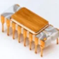
4004-powersmall-120x120 CHIPMAKER Intel today celebrates the 40th anniversary of the 4004, the world's first commercially available microprocessor.

To call Intel's 4004 just a microprocessor is to do the microelectronics world a great disservice. Not only was the Intel 4004 the first commercial microprocessor, shattering what people thought of computers, it signaled Intel's shift away from manufacturing memory and into what was going to become the industry that changed the world forever.

Back in 1969 when Japanese calculator outfit Nippon Calculating Machine Corporation asked Intel to design 12 chips for a business calculator called Busicom, Intel had already achieved some success with its memory business. Although Intel was far from being a market leader, the two 'Fairchildren', Robert Noyce and Gordon Moore were busy making money fabbing RAM chips, but not for much longer.

Back in 1969, Intel didn't have the luxury of saying no to business and Federico Faggin, Ted Hoff and Masatoshi Shima got to work on designing a processor for the relatively mundane business calculator. Later Hoff remarked that in the late 1960s it simply wasn't feasible to talk about personal computers.

Like the birth of many revolutionary pieces of engineering, the 4004 was designed by a bunch of engineers working into the night on the promise of creating something completely different.

While Faggin, who had also worked at Fairchild Semiconductor with Noyce and Moore, was busy designing the 4004 Hoff is widely credited with coming up with the architecture. Faggin built Hoff's architecture, with the legend saying that the first wafers came back to Intel's Santa Clara offices at 6PM just as everyone was clocking out for the day. Faggin pulled an all nighter in the lab to check whether the first baked 4004 actually worked, and at 3AM, overcome with exhaustion and satisfied that the radical 4004 did the job, he went home to tell his wife, "It works!".

Faggin was so proud of his design that he etched his initials, FF, on one side of the 4004's design. In later iterations of the 4004 the initials were moved, but just like an artist, Faggin signed his own work. And make no mistake, the 4004 processor is a work of art.

It might sound bashful, but Intel's 4004 wasn't particularly powerful, and the firm admitted, "The 4004 was not very powerful, it was primarily used to perform simple mathematical operations in a calculator called Busicom." However Noyce and Moore realised that it wasn't the 4004 itself that was important but its architecture.

4004-layout-185x299 In terms of complexity, Intel's 4004 had 2,300 MOS transistors and was fabricated on a 10,000nm process node on 60mm wafers. In a graphic illustration of Moore's law, processors from Intel and AMD today typically have hundreds of millions of transistors and are fabricated on the 32nm process node on 300mm wafers. But the numbers simply don't tell the whole story, the fact is that the 4004 was not just a new chip with a new micro-architecture, but it was a radical new way of thinking and building processors.

What Faggin, Hoff and Shima had created with the 4004 was the ability to commoditise computing by adding the micro in microprocessors. Prior to the 4004, general purpose computers were the hulking machines you saw in black-and-white films as room-sized equipment. Henry Ford brought the motorcar to the wider public through mass production, while Intel brought computing to the masses by miniaturising it.

Intel showed what would become perhaps the first known example of its shrewd business policies by offering Busicom, now a company in its own right, a reported $60,000 for the design and marketing rights for the 4004. Busicom agreed to the deal and, even though a year later the firm went bust, Intel was left with the ability to sell the 4004, which it did in 1971.

In what would become standard Intel behaviour, the firm courted developers for its 4004 processor. Even at that time, Intel knew that software held the key to its success, and it wasn't wrong.

Like Noyce and Moore, Faggin chose to form his own company in 1974 called Zilog. The firm is extremely successful in embedded CISC processors but is best known for producing chips that were found in the Sinclair ZX Spectrum. Faggin still heads up Zilog but his name will forever be associated with the creation of arguably the 20th century's most important innovation in electronics. Shima followed Faggin to Zilog in 1975 and worked on the Z80 and Z8000.

Hoff stayed on at Intel, becoming an Intel Fellow and more recently was awarded the National Medal of Technology and Innovation in 2009 by US President Barack Obama, a year before Faggin received the same award.

What Faggin, Hoff and Shima created wasn't just a microprocessor, it was a blueprint for others to follow and quite simply extended what was thought possible. Credit should be given to Noyce, Moore and Intel's third co-founder, Andy Grove, for letting the electronics engineers have the time and resources to develop what was perhaps the most important, ground-breaking electronic component created in the past century. µ

Wednesday, 9 November 2011

Silicon Blue launches 40nm fgpas

Programmable logic developer Silicon Blue is sampling the iCE40 mobileFPGA family, which includes devices targeted at smartphones and tablets. Fabricated on TSMC's 40nm low power standard cmos process, the LP and HX families provide twice the logic capacity of the company's 65nm iCE65 devices. "We've proven our technology leadership siliconblueFPGAwith iCE65 and are on track to ship approximately 10million units this year," said ceo Kapil Shankar. The LP series, aimed at smartphones, and the HX series, designed with tablets in mind, offer sensor management and high speed custom connectivity. Silicon Blue calls its technology Custom Mobile Devices (CMDs). There are five devices in both series, with capacities ranging from 640 to 16,192 logic cells. However, while the HX range offers higher performance, it consumes more power. Both versions come in 2.5 x 2.5mm micro plastic bgas, Shankar added: "We've taken the next bold step with CMDs by extending video performance capability for smartphones to 525Mbit/s, enabling HD720p 60Hz (1280 x 720) and HD1080p 30Hz (1920 x 1080). For tablets, CMDs can now support WUXGA (1920x1200) with dual LVDS, HD720p 60Hz (1280x720) and HD1080p 30Hz (1920x1080)."

Another 40nm family, code named San Francisco, will be announced later in 2011.