Featured post

Top 5 books to refer for a VHDL beginner

VHDL (VHSIC-HDL, Very High-Speed Integrated Circuit Hardware Description Language) is a hardware description language used in electronic des...

Thursday, 13 June 2013

How 450mm wafers will change the semiconductor industry

The semiconductor industry's transition to making chips on 450-millimeter wafers is better described as a "transformation," Jonathan Davis of Semiconductor Equipment and Materials International writes. "The shift to 450mm will take a several years to manifest and numerous complexities are being skillfully managed by multiple organizations and consortia," he writes, adding, "However, once the changeover occurs, in hindsight, most in the industry will recognize that they participated in something transformational."

Even for the segments that continue manufacturing semiconductor devices on 300mm and 200mm silicon wafers, the industry will change dramatically with the introduction of 450mm wafer processing. The 450mm era will impact industry composition, supply chain dynamics, capital spending concentration, future R&D capabilities and many other facets of today’s semiconductor manufacturing industry — not the least of which are the fabs, wafers and tools with which chips are made.

The shift to 450mm will take a several years to manifest and numerous complexities are being skillfully managed by multiple organizations and consortia.   For those reasons, the evolutionary tone of “transition” seems appropriate. However, once the changeover occurs, in hindsight, most in the industry will recognize that they participated in something transformational.

No transformation occurs in isolation and other factors will contribute to the revolutionary qualities of 450mm.  Market factors, new facilities design, next generation processing technology, the changing dynamics of node development and new materials integration will simultaneously affect the industry landscape.

While reading about the implications of 450mm is valuable, I believe that there is much to learn by being a part of the discussion. How is this future transformation being envisioned and acted on today?  I hope that you will join us — at our “live” event, where you will have the opportunity to hear first-hand information… direct from well-informed experts in the industry.

Potential revisions in the 450mm wafer specification are under consideration.  At least two issues are currently being evaluated by the industry and both portend significant ramifications for wafer suppliers, equipment makers and those technologies that interface with the wafer.

First, the wafer orientation method may be revised to eliminate the orientation “notch” on the perimeter of the substrate. The notch was introduced in the 300mm transition as an alternative to the flat.  However, both equipment suppliers and IC makers, through a constructive and collaborative dialog, have concluded that eliminating the notch can potentially improve the die yield, tool performance and cost.

Secondly, reduction of the wafer edge exclusion area — that peripheral portion of the silicon on which no viable device structure occurs — also offers potential yield advantages.  The current 450mm wafer specification (SEMI E76-0710), originally published in 2010, calls for a 2mm edge exclusion zone.  IC makers believe that reduction of this area to a 1.5mm dimension offers the cost equivalence of a 1 percent yield increase.  Though a percent may sound trivial, it is represents substantial increased value over time.

Along with cost and efficiency improvements, IC makers and consortia driving the transition to 450mm manufacturing expect to achieve similar or better environmental performance. Larger footprints and resource demands from 450mm facilities in conjunction with mandates for environmentally aware operations are compelling fabs and suppliers to consider sustainability and systems integration at greater levels than ever before.

Experts in fab facilities, energy, water and equipment engineering will discuss the implications of 450mm to environment, health and safety during the SEMICON West 450mm Manufacturing EHS Forum on Wednesday, July 10.

Included in the presentations are perspectives from the Facility 450 Consortium (F450C) including Ovivo, Edwards and M+W Group.  A holistic Site Resource Model that provides semiconductor manufacturers visibility into effective reduction of total energy and water demands for individual systems, as well as for the entire facility will be reviewed by CH2M Hill. The model is an integrated analytical approach to assess and optimize a semiconductor facility’s thermal energy, electrical energy, and water demand, as well as the cost associated with these resources.

Saturday, 1 June 2013

Keep Environment Variables when Using SUDO

Recently we were developing a script in perl where we need to specify the environment variable UVM_LIBRARY_PATH = ../examples/UVM1.10, but when we run the code with sudo script/server, it doesn't run because that library path is not in root's env.

Its very easy to keep the env variables even while running the script with SUDO. All you need to do is modify your /etc/sudoers file

search following lines

Defaults    env_reset
Defaults env_keep = "COLORS DISPLAY HOSTNAME HISTSIZE INPUTRC KDEDIR \
LS_COLORS MAIL PS1 PS2 QTDIR USERNAME \
LANG LC_ADDRESS LC_CTYPE LC_COLLATE LC_IDENTIFICATION \
LC_MEASUREMENT LC_MESSAGES LC_MONETARY LC_NAME
LC_PAPER LC_TELEPHONE LC_TIME LC_ALL LANGUAGE LINGUAS \
_XKB_CHARSET XAUTHORITY"

Add env variable eg. UVM_LIBRARY_PATH. in our case we have

Defaults    env_keep = "COLORS DISPLAY HOSTNAME HISTSIZE INPUTRC KDEDIR \
LS_COLORS MAIL PS1 PS2 QTDIR USERNAME \
LANG LC_ADDRESS LC_CTYPE LC_COLLATE LC_IDENTIFICATION \
LC_MEASUREMENT LC_MESSAGES LC_MONETARY LC_NAME
LC_PAPER LC_TELEPHONE LC_TIME LC_ALL LANGUAGE LINGUAS \
_XKB_CHARSET XAUTHORITY UVM_LIBRARY_PATH"

Save your file and run the script.


Get free daily email updates!


Follow us!


Saturday, 18 May 2013

flexible heart monitor thinner than a dollar bill

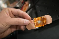
12625-babyskin_news Stanford Engineers combine layers of flexible materials into pressure sensors to create a wearable heart monitor thinner than a dollar bill. The skin-like device could one day provide doctors with a safer way to check the condition of a patient's heart.

Most of us don't ponder our pulses outside of the gym. But doctors use the human pulse as a diagnostic tool to monitor heart health.

Zhenan Bao, a professor of chemical engineering at Stanford, has developed a heart monitor thinner than a dollar bill and no wider than a postage stamp. The flexible skin-like monitor, worn under an adhesive bandage on the wrist, is sensitive enough to help doctors detect stiff arteries and cardiovascular problems.

The devices could one day be used to continuously track heart health and provide doctors a safer method of measuring a key vital sign for newborn and other high-risk surgery patients.

Read More >>

Get free daily email updates!

Follow us!

Linux/Unix - Search and remove files with one find command on fly

Some time it is necessary to find out files and remove them as we need to do today. However, rm command does not support search criteria.

However, with find command you can search for files in a directory and remove them on fly.

You need to combine find and rm command together.

Fortunately find command makes this operation quite easy.

You can use find command as follows:

find . -type d -print | grep <file_name/dir_name> | xargs -n1 rm -rf

Get free daily email updates!

Follow us!

Wednesday, 24 April 2013

UI scientists create powerful microbatteries

UI …. i.e. University of Illinois…

IonCrossing_in_new_battery Developed by researchers at the University of Illinois at Urbana-Champaign, the new microbatteries out-power even the best supercapacitors and could drive new applications in radio communications and compact electronics.

The most powerful batteries on the planet are only a few millimeters in size, yet they pack such a punch that a driver could use a cellphone powered by these batteries to jump-start a dead car battery – and then recharge the phone in the blink of an eye.

“This is a whole new way to think about batteries. A battery can deliver far more power than anybody ever thought. In recent decades, electronics have gotten small. The thinking parts of computers have gotten small. And the battery has lagged far behind. This is a microtechnology that could change all of that. Now the power source is as high-performance as the rest of it,” said William P. King, bliss professor of mechanical science and engineering.

“The picture illustrates a high power battery technology from the University of Illinois.  Ions flow between three-dimensional micro-electrodes in a lithium ion battery.”

With currently available power sources, users have had to choose between power and energy. For applications that need a lot of power, like broadcasting a radio signal over a long distance, capacitors can release energy very quickly but can only store a small amount. For applications that need a lot of energy, like playing a radio for a long time, fuel cells and batteries can hold a lot of energy but release it or recharge slowly.

The new microbatteries offer both power and energy, and by tweaking the structure a bit, the researchers can tune them over a wide range on the power-versus-energy scale.

The batteries owe their high performance to their internal three-dimensional microstructure. Batteries have two key components: the anode (minus side) and cathode (plus side). Building on a novel fast-charging cathode design by materials science and engineering professor Paul Braun’s group, King and Pikul developed a matching anode and then developed a new way to integrate the two components at the microscale to make a complete battery with superior performance.

The graphic illustrates a high power battery technology from the University of Illinois.  Ions flow between three-dimensional micro-electrodes in a lithium ion battery.

With so much power, the batteries could enable sensors or radio signals that broadcast 30 times farther, or devices 30 times smaller. The batteries are rechargeable and can charge 1000 times faster than competing technologies – imagine juicing up a credit-card-thin phone in less than a second. In addition to consumer electronics, medical devices, lasers, sensors and other applications could see leaps forward in technology with such power sources available.

“Any kind of electronic device is limited by the size of the battery – until now. Consider personal medical devices and implants, where the battery is an enormous brick, and it’s connected to itty-bitty electronics and tiny wires. Now the battery is also tiny,” explained Mr. King.

Now, the researchers are working on integrating their batteries with other electronics components, as well as manufacturability at low cost.

“To dare is to lose one's footing momentarily. To not dare is to lose oneself.”

Get free daily email updates!

Follow us!

Wednesday, 17 April 2013

Xilinx enables C programmable FPGAs

Vivado_xilinx The Vivado Design Suite 2013.1 includes a new IP-centric design environment designed to accelerate system integration, and a set of libraries to accelerate C/C++ system-level design and high-level synthesis (HLS). The update provides a workflow that does not dictate how a design team works.

Users of Vivado HLS can access video processing functions integrated into an OpenCV environment for embedded vision running on the dual-core ARM processing system.

It delivers, says Xilinx, up to a 100X performance improvement of existing C/C++ algorithms through hardware acceleration.

Read more…

Get free daily email updates!

Follow us!

Tuesday, 16 April 2013

India needs homegrown wafer fabs for its electronics

FAB_VLSI The government of India is offering up to $2.75 billion in incentives for the construction and equipping of the country's first wafer fabrication facility. India imported $8.2 billion in semiconductors last year, according to Gartner. Getting its own wafer fab is said to present a number of challenges to India, especially in the necessary infrastructure and an ecosystem of suppliers.

The domestic purchasing mandate, known as the “preferential market access” policy, seeks to address a real problem: imports of electronics are growing so fast that by 2020, they are projected to eclipse oil as the developing country’s largest import expense.

India’s import bill for semiconductors alone was $8.2 billion in 2012, according to Gartner, a research firm. And demand is growing at around 20 percent a year, according to the Department of Electronics and Information Technology.

For all electronics, India’s foreign currency bill is projected to grow from around $70 billion in 2012 to $300 billion by 2020, according to a government task force.

Read more…

Get free daily email updates!

Follow us!